Overview
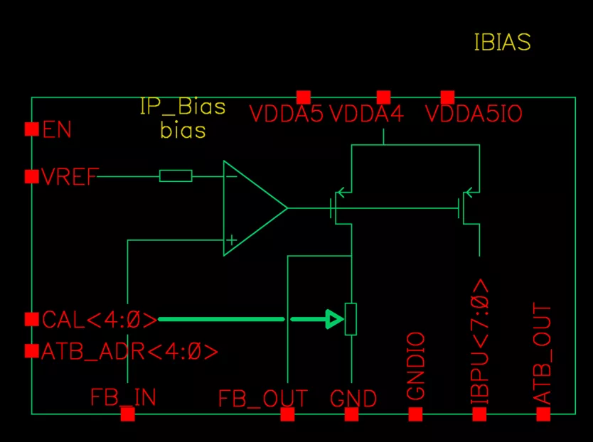
The TS_CS_20uA_X8 is a current generator sourcing 20µA via each terminal IBPU<0> through IBPU<7>, for the biasing of other TES IPs like TS_FS_9M70_X8 and TS_VA_LNDC_X8 (for the latter IP, its input reference current must be mirrored from one Bias output by a simple cascoded NMOS circuit).
The Bias operates with two supply voltages, VDDA4 (4V typical) for its main function and VDDA5, VDDA5IO (5V typical) for the test-bus (ATB) circuit. It requires one precision reference voltage VREF (2.5V).
Precision current trimming is achieved under control of the 5-bit calibration input CAL<4:0>.
This IP supports analog-test-bus multiplexing on the ATB_OUT output under control of the 5-bit address input ATB_ADR<4:0>. When ATB_ADR<4:0>= LLLHH, the Bias sources a 20µA current replica to ATB_OUT for off-chip measurement.
This IP complies with 2kV electrostatic discharges on its analog terminal ATB_OUT.
The minimum continuous operation lifetime spans 100000 hours.
Operating conditions
| Parameters |
Values |
| Junction temperature range |
20ºC to +80ºC |
| Supply voltages |
VDDA5, VDDA5IO: 4.9V to 5.1V ; VDDA4: 3.9V to 4.1V (supplied by the additional IP TS_VR_4V00_X8) |
| Reference voltage |
VREF: 2.5V |
| Voltage at IBPU<7:0> terminals |
2V max |
| EN, CAL<4:0> logic-high voltage level |
VDDA4 |
| ATB_ADR<4:0> logic-high voltage level |
VDDA5 |
Specification
| Parameters |
Values |
| Calibrated output bias current intensity per IPBU output |
20.0µA±0.5µA |
| Start-up time |
2µs max |
| PSRR over frequencies from DC up to 10 MHz |
5%/V max |
| Operating power consumption with unused IBPU<7:0> |
765µW max |
| Powerdown-mode current consumption Enable EN low |
11nA max |
| Area |
0.031mm² |
FB_IN and FB_OUT must be interconnected.
Learn more about Voltage Reference IP core
TES Electronic Solutions GmbH announces the availability of TS_XOSC_32k_X8, a low-power 32.768 kHz Pierce crystal oscillator IP designed to provide a reliable low-frequency timing reference for battery-powered ASICs and system-on-chip (SoC) applications.
TES Electronic Solutions GmbH announces the availability of its DC-DC converter IP, TS_SWC_DCDC_3V6_X8, a 3.6 V boost‑buck converter that can be powered from a 2.5 V - 5.5 V supply voltage.
To meet the growing graphics demands, the industry is shifting toward scalable, shader programmable architectures. Unlike fixed-function graphics accelerators, shader programmable GPUs offer the flexibility required to target diverse market segments and at the same time ensure software portability and maintainability. Furthermore, adopting platform-independent stacks based on industry standards allows accelerating time-to market by developing applications on standard PC platforms before deployment to target hardware. TES Electronic Solutions in Germany addresses these challenges with the D/AVE NX GPU core. Engineered specifically for resource-constrained environments, it supports OpenGL ES 2.0 shader programmability with selected 3.x and vector graphics extensions.
TES Electronic Solutions GmbH offers TS_OVLO_3V3_X8 which is a compact Over-Voltage Lockout (OVLO) IP designed to protect battery-powered electronic systems against over-voltage and reverse-polarity faults of up to ±30 V.
A new DC-DC Split-Pi Boost-Buck Converter IP is released to offer designers a simple way to achieve high efficiency and precise regulation. TS_SPLITPI_3V3_X8 is a cascaded 3.3 V boost‑buck converter that can be powered from either a 10 V - 30 V supply or a low-voltage backup battery.
TES Electronic Solutions GmbH offers two new voltage buffer IPs with driving capabilities up to 6 mA, built on X-FAB’s XT018-0.18µm BCD-on-SOI process and operate across a junction temperature range of -40°C to 150°C with a supply voltage of 3.2V to 3.4V.