ONFI 5.2: What’s new in Open NAND Flash Interface's latest 5.2 standard
ONFI 5.2 is the latest generation of ONFI device standard, published in 2024. ONFI 5.2 devices have added several major features over previous generation ONFI standards.
The EP501 NAND Flash controller provides an easy interface for user to access single-level and multi-level cell (SLC and MLC) NAN…
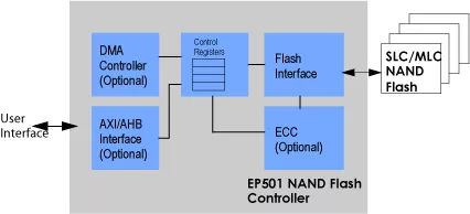
The EP501 NAND Flash controller provides an easy interface for user to access single-level and multi-level cell (SLC and MLC) NAND Flash devices. NAND Flash devices are accessed through complicated sequence of command, address, data, and confirmation protocols. The EP501 manages all the hardware protocols and allows the user to access NAND Flash memory simply by reading and writing control registers of the EP501.
A very large size of NAND Flash memory can be accessed through a small number of control registers. The NAND Flash controller occupies only a small size in the system’s memory space without scarifying system performance. Burst access to the NAND Flash memory is supported by the controller at full memory bandwidth. Timing parameters of the controller is fully programmable so different memory speeds are supported regardless of the operating frequency of the controller.
Hardware generated ECC provides the required ECC protection for NAND Flash devices. For SLC NAND Flash, the EP501 support Hamming Code for single bit correction and double bit detection. For MLC devices, the EP501 can be available with Bose, Chaudhuri, and Hocquenghem (BCH) code for multi-bit ECC error. User has the choice of 4-bit or 8-bit protection per 512 bytes of user data.
The EP501 includes many features to improve system performance and increase system design flexibility. The Boot ROM support feature automatically open a page of the NAND Flash device upon reset. This allows the host CPU can execute directly from the NAND Flash device’s first page. Furthermore, a built-in DMA controller can transfer Boot page data to system memory and CPU can execute from system memory.
The Write-Trigger-Read feature allows the user to open a page of the NAND Flash device for read by writing a special code to the command register. Writing to command register takes very few cycles on the user interface, thus frees the host CPU to execute other tasks while waiting for the page to be open.
The Two-Plane program and erase procedure common found in large NAND Flash device is also supported by the controller. The two-plane operation allows two planes to be programmed or erase at the same time, thus double the data bandwidth of the NAND Flash device.
Several options of user interface are available for the user to choose from. The standard version features a simple user interface that is designed for on-chip system integration. It has separate address and data buses and command signals that supports burst transfer and wait state insertion. Standard interface buses including AXI, AHB, Wishbone and Avalon bus are available. The controller acts as a target or slave device on these buses. With these standard bus interfaces, the EP501 can be integrate seamlessly with systems built on these standards.
Note: some files may require an NDA depending on provider policy.

NAND Flash Controller is a NAND Flash IP core from Eureka Technology, Inc. listed on Semi IP Hub.
Engineers should review the overview, key features, supported foundries and nodes, maturity, deliverables, and provider information before shortlisting this NAND Flash IP.
Yes. Buyers can compare this product with similar semiconductor IP cores or IP families based on category, provider, process options, and structured technical specifications.