Vendor: Eureka Technology, Inc. Category: NAND Flash

Synchronous ONFI NAND Flash Controller
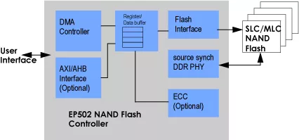
Synchronous ONFI NAND Flash Controller

Key features

  • Supports single-level and multi-level cells (SLC and MLC) NAND Flash devices.
  • Compatible with ONFI 2.1 Flash Interface for synchronous and asynchronous access.
  • Supports source synchronous double data rate data transfer for highest possible data bandwidth.
  • Supports 2k and 4k page sizes.
  • Simple user interface designed for easy on-chip integration.
  • Choices of AHB, AXI, Wishbone and Avalon user interface.
  • Built-in DMA engine for autonomous data transfer.
  • Internal data buffer to maximize data bandwidth.
  • Optional ECC correction with BCH code for 4, 8, 12 or more error bits per 512 bytes.
  • Stores ECC code in spare column area.
  • Write-triggered read operation eliminates long wait states when open a new page,
  • Enable NAND Flash to be used as BOOT ROM.
  • Compatible with standard FTL software and Linux JFFS2 for wear leveling and bad block management.
  • Designed for ASIC and FPGA implementation
  • Differentiating Features
    • Choices of AHB, AXI, PLB, Wishbone and Avalon user interface.
    • Hamming code and BCH ECC.
    • Built in DMA Controller for boot code and data transfer.

Block Diagram

Specifications

Identity

Part Number
EP502
Vendor
Eureka Technology, Inc.
Type
Silicon IP
Controller / PHY
Controller

Files

Note: some files may require an NDA depending on provider policy.

Provider

Learn more about NAND Flash IP core

Concealable physical unclonable functions using vertical NAND flash memory

Here, the authors propose a concealable PUF using V-NAND flash memory by generating PUF data through weak Gate-Induced-Drain-Leakage (GIDL) erase. The differences in doping depth among V-NAND strings arising from the fabrication cause variations in GIDL erase performance. The resulting V-NAND PUF demonstrated ideal security characteristics while maintaining 100% accuracy under variations in read count and temperature.

Scaling NAND flash to 20-nm node and beyond

Intel-Micron have recently introduced a scalable planar NAND cell for the 20nm technology [1]. Replacement of conventional wrap floating gate (FG) NAND memory cell with a High-K/Metal gate planar cell that can scale to the 20nm node and beyond was a significant challenge and required comprehensive material and cell exploration and optimization. This paper discusses some of the fundamental cell design issues considered and addressed to arrive at this planar cell technology including the reasoning behind choosing the planar floating gate cell over the nano-crystal cell, and the nitride cell.

Frequently asked questions about NAND Flash Interface IP

What is Synchronous ONFI NAND Flash Controller?

Synchronous ONFI NAND Flash Controller is a NAND Flash IP core from Eureka Technology, Inc. listed on Semi IP Hub.

How should engineers evaluate this NAND Flash?

Engineers should review the overview, key features, supported foundries and nodes, maturity, deliverables, and provider information before shortlisting this NAND Flash IP.

Can this semiconductor IP be compared with similar products?

Yes. Buyers can compare this product with similar semiconductor IP cores or IP families based on category, provider, process options, and structured technical specifications.

×
Semiconductor IP