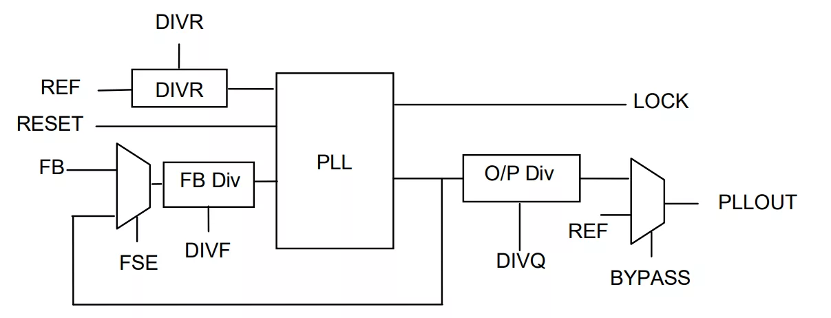
Overview
The low-power wide range PLL addresses markets and applications that demand very low power and optimized for area efficiencies. In addition, consumer devices have restrictions on supply voltage due to battery restrictions or board restrictions. The PLLs also needs to be designed on standard digital logic processes and expected to work in noisy SoC environments.
The PLL macro is implemented in Analog Bits’ proprietary architecture that uses core supply only. The PLL resides inside the IO ring that includes two analog power supply pads, occupying no core area. In order to minimize noise coupling and maximize ease of use, the PLL incorporates a proprietary ESD structure, which is proven in several generations of processes. Eliminating band-gaps and integrating all on-chip components such as capacitors and ESD structures, helps the jitter performance significantly and reduces stand-by power. The PLL macro fits into any standard IO pad pitch and can be implemented in staggered and in-line IO configurations.
PLL Operational Range Description Symbol Min Typ Max Units Input Frequency FREF 5 140 MHz Post-Divide Reference Frequency FPFD 5 140 MHz VCO Frequency FVCO 800 MHz Output Frequency FOUT 12.5 400 MHz Output Duty Cycle tDO 45 55 % Total area of macro (excluding bond pad area) A 0.024 sq. mm May vary depending on size of IO slots Chip core area requirement CA 0 sq. mm Total Power IDD 0.8 mA Operational Voltage (Digital) VDIG 1.08 1.2 1.32 V Operational Voltage (Analog) VANA 1.08 1.2 1.32 V Operational Temperature TOP -40 25 125 C Table 1: PLL Operational Range
Learn more about PLL IP core
At TSMC 2026 North America OIP Ecosystem Forum, Analog Bits will showcase new real-time power observability and sensing analog IP in TSMC’s N2P process technology and present a paper with Cerebras; Papers planned with partners at global OIP Ecosystem events to highlight smarter power delivery for scalable SoCs targeting data centers, automotive and more.
Strategic investment strengthens worldwide engineering capabilities and accelerates innovation to support growing need for smarter and more efficient analog and power solutions for advanced semiconductors.
Analog Bits continues to develop innovative mixed signal IP in TSMC N2P process technology, with integrated LDOs, pinless remote PVT sensors, and microwatt class and high-performance LC PLLs
We are honored to receive the 2025 OIP Partner of the Year Award from TSMC in the Analog IP category for enabling customer designs with broad portfolio of IPs to accelerate design creation.
Company will demonstrate newest LDOs, PLLs, and sensors proven on TSMC’s latest process technologies at the TSMC 2025 Open Innovation Platform® (OIP) Ecosystem Forum in Silicon Valley
Analog Bits will be demonstrating its newest LDO, power supply droop detectors, embedded clock LC PLL’s on the TSMC N3P process, and clocking, high-accuracy PVT and droop detectors on the TSMC N2P process at the Analog Bits booth at the TSMC 2025 North America Technology Symposium in Santa Clara, California.