High Speed Wide Range PLL on GLOBALFOUNDRIES 65G
The high speed wide range PLL addresses markets and applications that demand very low power and optimized for area efficiencies.
Overview
The high speed wide range PLL addresses markets and applications that demand very low power and optimized for area efficiencies. In addition, consumer devices have restrictions on supply voltage due to battery restrictions or board restrictions. The PLLs also needs to be designed on standard digital logic processes and expected to work in noisy SoC environments.
The PLL macro is implemented in Analog Bits’ proprietary architecture that uses core and 2.5V IO devices.
The PLL resides inside the IO ring of two analog power supply pads, occupying no core area. In order to minimize noise coupling and maximize ease of use, the PLL incorporates a proprietary ESD structure, which is proven in several generations of processes. Eliminating band-gaps and integrating all on-chip components such as capacitors and ESD structures, helps the jitter performance significantly and reduces stand-by power.
The PLL macro fits into any standard IO pad pitch and is available for both staggered and in-line IOs.
PLL Operational Range Description Symbol Min. Typ. Max. Units Input frequency FREF 10 800 MHz Post-Divide Reference Frequency FPFD 10 200 MHz VCO Frequency FVCO 2000 MHz Output Frequency FOUT 10 2000 MHz Output Duty Cycle (FOUT <=1000MHz) tDO 45 55 % Output Duty Cycle (FOUT >1000MHz) tDO 40 60 % Total area of macro (excluding bond pad area) A 0.022 sq.mm Depends on size of IO slots Chip core area requirement CA 0 sq.mm Total Power IDD 2 mA Operational Voltage (Digital) VDIG 0.9 1.0 1.1 V Operational Voltage (Analog) (uses 2.5V IO) VANA 2.25 2.5 2.75 V (options available for other IO voltages) Operational Temperature TOP -40 25 125 C Table 1: PLL Operational Range
Key features
- Electrically Programmable PLL for multiple applications
- Wide Ranges of Input and Output Frequency for diverse clocking needs
- Implemented with Analog Bits’ proprietary architecture
- Fully integrated inside industry standard or other customized IO ring
- Occupies zero core area
- Spread Spectrum tracking capability
- Requires no additional on-chip components or band-gaps, minimizing power consumption
- Excellent jitter performance with optimized noise rejection
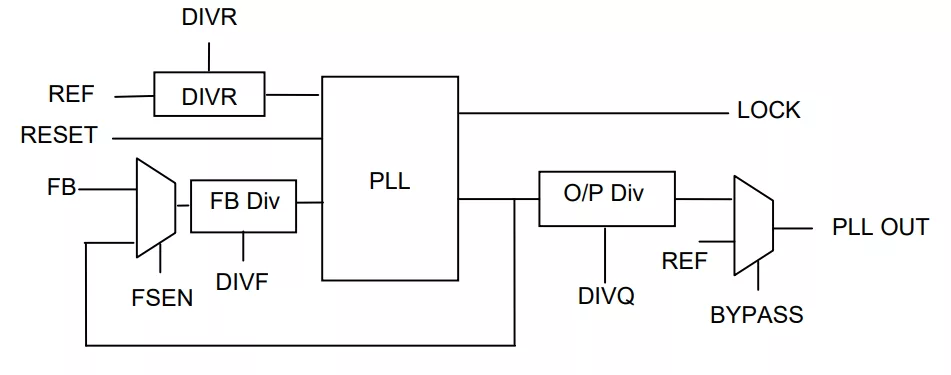
Block Diagram
Silicon Options
| Foundry | Node | Process | Maturity |
|---|---|---|---|
| GlobalFoundries | 65nm | G | — |
Specifications
Identity
Files
Note: some files may require an NDA depending on provider policy.
Provider
Learn more about PLL IP core
CoreHW Develops 80GHz mmWave PLL with Synopsys RFIC Design Flow on GlobalFoundries 22FDX Technology
Specifying a PLL Part 3: Jitter Budgeting for Synthesis
Specifying a PLL Part 2: Jitter Basics
Specifying a PLL Part 1: Calculating PLL Clock Spur Requirements from ADC or DAC SFDR
Achieving Groundbreaking Performance with a Digital PLL
Frequently asked questions about PLL IP cores
What is High Speed Wide Range PLL on GLOBALFOUNDRIES 65G?
High Speed Wide Range PLL on GLOBALFOUNDRIES 65G is a PLL IP core from Analog Bits Inc. listed on Semi IP Hub. It is listed with support for globalfoundries.
How should engineers evaluate this PLL?
Engineers should review the overview, key features, supported foundries and nodes, maturity, deliverables, and provider information before shortlisting this PLL IP.
Can this semiconductor IP be compared with similar products?
Yes. Buyers can compare this product with similar semiconductor IP cores or IP families based on category, provider, process options, and structured technical specifications.