
Digital and mixed-signal IP and ASIC RISC-V reference design for USB Type-C/PD power adapter/charger
IQonIC Works USB-C/PD power adapter IP includes components required to build an integrated programmable power supply (PPS) charge…
Overview
IQonIC Works USB-C/PD power adapter IP includes components required to build an integrated programmable power supply (PPS) charger solution.
The USB Type-C source controller detects connections and controls provision of VBUS and VCONN power.
The USB BC and QuickCharge controller negotiates power supply for legacy devices using BC1.2 and QC2/3/4 protocols.
The USB PD controller autonomously negotiates power contracts with a device using PD 2.0 or 3.0 protocols, including PPS messaging. It includes PHY, protocol, and source policy layers, and integrates with a host processor that provides device policy management.
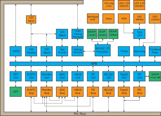
The usb_pa_platform reference design integrates these IP blocks with other IQonIC Works IP into a complete power adapter ASIC solution. The platform includes power-supply control using an IDAC, VBUS load switch control, ADC, fault monitoring, temperature sensing, a RISC-V processor subsystem with ROM/OTP/SRAM memory, and I2C and GPIO interfaces.
IQonIC Works provides embedded firmware for the usb_pa_platform. The firmware can be customized for a target application using IQonIC Works IDE, which integrates with the embedded debugger in the hardware platform.
Key features
- RISC-V RV32EC processor subsystem with debug module, JTAG debug transport, and instruction and data ROM and SRAMs
- Bandgap Vref/Ibias blocks that provide reference voltage and bias currents to analog blocks
- LDOs to derive power from the the external converter to power internal digital logic, analog blocks, and I/Os
- Power-on (PON) reset for digital blocks during power-supply ramp up and down
- 48MHz oscillator that provides the main clock for digital blocks
- 10kHz low power oscillator that provides a clock for the watchdog timer
- System control block that provides clock and reset control for digital logic, including clock gating
- System timer and watchdog timer
- I2C slave interface for test-access
- I2C slave controller for external host access
- I2C master interface for general purpose use
- I2C transceivers
- GPIO controller for outputs
- USB PD control and analog transceiver. The PD control implements PHY, protocol, and source policy engine layers.
- USB Type-C control and analog front end. The Type-C control implements the source state diagram.
- USB BC1.2 and QuickCharge 2/3/4 control and analog front end
- Power supply (PS) control and analog front end to control the setpoint for the external regulator, including slew-rate controlled transitions between voltages
- Current sense (ISNS) amplifier and control
- VBUS control and analog front end, including load-switch gate driver, discharge resistor, and voltage divider for VBUS measurement
- Monitoring control and analog front end for over-voltage, over-current, and reverse-current protection. The block includes comparators and interrupt request logic for fast response to faults.
- NTC thermistor and configuration resistor control and analog front end, driving source current into external resistors to generate a voltage to be measured by the ADC
- Multichannel SAR ADC control and analog front end, used to measure power supply voltage, VBUS voltage, current sense, thermistor temperature, and config resistor voltages
- One-time programmable (OTP) memory with controller for programming and read access
- Test access port with I2C slave interface
- Test control and trim registers
- Flexible Licensing Options
- Project based, Term, or Perpetual Licenses (Single Project or Multi-Project, Single Technology or Multi-Project/Multi-Technology)
- Manufacturing License options (GDS IP)
Block Diagram
Applications
- USB-C/PD Source-only port
- Battery charger
What’s Included?
- Detailed data sheet and integration guide
- Synthesizable Verilog RTL source code
- ASIC digital synthesis constraints
- Complete analog IP in GDSII, including analog PHY
- FW source code
- FPGA development board with analog mezzanine card
- UVM based verification environment and test cases
- Design guide, programming user manual, and verification guide
Silicon Options
| Foundry | Node | Process | Maturity |
|---|---|---|---|
| GlobalFoundries | 130nm | BCD | — |
Specifications
Identity
Compute
Files
Note: some files may require an NDA depending on provider policy.
Provider
Learn more about CPU IP core
Announcing Arm AGI CPU: The silicon foundation for the agentic AI cloud era
ChiPy®: Bridge Neural Networks and C++ on Silicon — Full Inference Pipelines with Zero CPU Round-Trips
Unleashing Leading On-Device AI Performance and Efficiency with New Arm C1 CPU Cluster
Encarsia: Evaluating CPU Fuzzers via Automatic Bug Injection
Introducing Cortex-A320: Ultra-efficient Armv9 CPU Optimized for IoT
Frequently asked questions about CPU IP cores
What is Digital and mixed-signal IP and ASIC RISC-V reference design for USB Type-C/PD power adapter/charger?
Digital and mixed-signal IP and ASIC RISC-V reference design for USB Type-C/PD power adapter/charger is a CPU IP core from IQonIC Works listed on Semi IP Hub. It is listed with support for globalfoundries.
How should engineers evaluate this CPU?
Engineers should review the overview, key features, supported foundries and nodes, maturity, deliverables, and provider information before shortlisting this CPU IP.
Can this semiconductor IP be compared with similar products?
Yes. Buyers can compare this product with similar semiconductor IP cores or IP families based on category, provider, process options, and structured technical specifications.