Differential Clock Receiver - Samsung SF2A
Differential Clock Receiver on Samsung SF2A
Overview
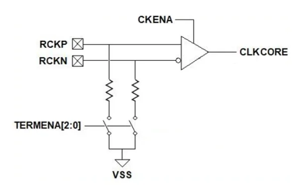
Analog Bits’ Differential Clock Receiver macro is a receiver including on-chip termination, and addresses a large portfolio of applications. The Receiver is designed for digital logic processes and use robust design techniques to work in noisy SoC environments, ranging from high-speed communication to low power consumer applications.
The Receiver macro is implemented in Analog Bits’ proprietary architecture that uses core devices operated at core voltage. In order to minimize noise coupling and maximize ease of use, the Receiver incorporates proprietary ESD structures, which is proven in several generations of processes.
Receiver Operational Range
| Description | Symbol | Min | Typ | Max | Units |
|---|---|---|---|---|---|
| Input Frequency | FCLK | 1 | — | 600 | MHz |
| Input Duty Cycle | DIN | 40 | — | 60 | % |
| Differential Input Voltage | VID | 0.2 | — | 0.8 | V |
| Common Mode Voltage | VCMR | — | 0 | — | V |
| Single Ended On Die Pull-down Termination (see table below) | R | — | — | — | Ω |
| Input Pad Skew | TSKEW | −50 | — | 50 | ps |
| Input Rise/Fall Time | tr/tf | 30 | 150 | 600 | ps |
| Area | A | — | 0.0082 | — | mm² |
| Total Power | IDD | — | 2.7 | 6.0 | mW |
| Operational Voltage (Analog) | VDD | 0.63 | 0.7 | 0.77 | V |
| Operational Temperature | TOP | −40 | 25 | 125 | °C |
Termination Configuration
| TERMENA[2:0] | Min (Ω) | Typ (Ω) | Max (Ω) |
|---|---|---|---|
| 000 (no termination) | — | — | — |
| 001 | 40 | 50 | 60 |
| 010 | 80 | 100 | 120 |
| 011 | 125 | 150 | 186 |
| 1xx | 160 | 200 | 240 |
Key features
- Differential clock receiver with single-ended output to chip core
- Wide Ranges of input frequencies for diverse clocking needs
- Core voltage only operation
- Low power consumption
- Programmable termination
- Built-in hysteresis
- Spread Spectrum tracking capability
- Requires no additional on-chip components or band-gaps, minimizing power consumption
- Implemented with Analog Bits’ proprietary architecture
- Designed for AEC-Q100 Automotive Grade 2 operation
Block Diagram
Silicon Options
| Foundry | Node | Process | Maturity |
|---|---|---|---|
| Samsung | 2nm | SF2A | Available on request |
Specifications
Identity
Provider
Learn more about High-Speed IP core
Analog Bits Expands Global Engineering Footprint with New Design Center in Dongtan, South Korea
Analog Bits Demonstrates Real-Time On-Chip Power Sensing and Delivery on TSMC N2P Process at TSMC 2026 Technology Symposiums
Analog Bits Awarded TSMC's 2025 OIP Partner of the Year Award
Analog Bits Adds New Power and Energy Management IP Blocks Proven on TSMC N2P and N3P Processes at TSMC 2025 OIP Ecosystem Forum
Analog Bits to Demonstrate IP Portfolio on TSMC 3nm and 2nm Processes at TSMC 2025 Technology Symposium
Frequently asked questions about High-Speed I/O Pad IP
What is Differential Clock Receiver - Samsung SF2A?
Differential Clock Receiver - Samsung SF2A is a High-Speed IP core from Analog Bits Inc. listed on Semi IP Hub. It is listed with support for samsung Available on request.
How should engineers evaluate this High-Speed?
Engineers should review the overview, key features, supported foundries and nodes, maturity, deliverables, and provider information before shortlisting this High-Speed IP.
Can this semiconductor IP be compared with similar products?
Yes. Buyers can compare this product with similar semiconductor IP cores or IP families based on category, provider, process options, and structured technical specifications.