TSMC N3P 1.2V High-Speed Test IO
The AI and HPC industries are advancing toward chiplet-based designs to achieve superior performance, as traditional monolithic S…
Overview
The AI and HPC industries are advancing toward chiplet-based designs to achieve superior performance, as traditional monolithic SoCs face scaling challenges. Heterogeneous integration is driving semiconductor innovation but adds complexity to chip design, requiring advanced testing methodologies and improved Automated Test Equipment (ATE). Increasing test patterns and limited package pins demand high-bandwidth IOs, while advancements in ATE capabilities further necessitate optimized GPIOs to support higher-speed, efficient and low-cost testing.
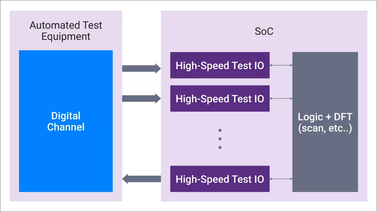
Synopsys High-Speed Test IO IP is a cutting-edge IO interface solution that enables efficient, high-speed testing of complex semiconductor designs while minimizing hardware complexity and cost. It achieves this by supporting high data rates (up to 2.5Gbps) for testing, reusing limited package pins for multiple modes (serving as test ports during manufacturing, enabling high-speed clock observation during debugging, and functioning as GPIO during production), and eliminating the need for complex protocols or calibration sequences. This simplifies testing, reduces development time and costs, and ensures high test coverage and reliability for advanced AI, HPC, and chiplet-based designs.
Key features
- High-Speed Data Transfer: Achieves data transfer rates of up to 2.5Gbps, for efficient testing during manufacturing
- Signal Integrity and Energy Efficiency: Maintains stable, high-speed performance while conserving energy with a low-power GPIO mode
- Simplified Testing Process: Protocol free solution, eliminates the need for initialization, calibration, and protocol support, streamlining hardware and software integration.
- Cost-Effective Design: Features a single-ended IO design that reduces area and cost without compromising performance
- Flexible Placement and Scalable Architecture: Modular design supports flexible IO placement and scalability for diverse chiplet-based SoC designs
- Multiplexed Functionality: Combines high-speed testing, clock observation, and GPIO functionality into a single, cost-effective interface
- Comprehensive Test Coverage: Supports BIST and Scan Test for thorough validation of complex semiconductor designs
Block Diagram
Silicon Options
| Foundry | Node | Process | Maturity |
|---|---|---|---|
| TSMC | 3nm | N3P | — |
Specifications
Identity
Files
Note: some files may require an NDA depending on provider policy.
Provider
Learn more about High-Speed IP core
Reduce Integration Risks for High-Speed Applications with PCIe 5.0-Compliant Synopsys IP
Addressing Signal and Power Integrity for High-Speed Data Center Applications
Synopsys Advances Die‑to‑Die Connectivity with 64G UCIe IP Tape‑Out
Synopsys Delivers First Complete UFS 5.0 and M‑PHY v6.0 IP Solution for Next‑Gen Storage
Securing UALink: Introducing Synopsys UALinkSec_200 Security Module
Frequently asked questions about High-Speed I/O Pad IP
What is TSMC N3P 1.2V High-Speed Test IO?
TSMC N3P 1.2V High-Speed Test IO is a High-Speed IP core from Synopsys, Inc. listed on Semi IP Hub. It is listed with support for tsmc.
How should engineers evaluate this High-Speed?
Engineers should review the overview, key features, supported foundries and nodes, maturity, deliverables, and provider information before shortlisting this High-Speed IP.
Can this semiconductor IP be compared with similar products?
Yes. Buyers can compare this product with similar semiconductor IP cores or IP families based on category, provider, process options, and structured technical specifications.