Overview
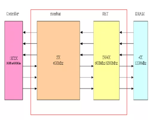
The DDR4/3 PHY is compatible with JEDEC DDR3 and JEDEC DDR4 SDRAMs, supports a range of DDR3 DRAM speeds from 666Mbps to 2133Mbps and DDR4 DRAM speeds from 1866Mbps to 2400Mbps, and target support x16 DDR3/DDR4 SDRAM components, the design include an analog hard macro (CLK/CMD/ADDR/DQ/DQS) and a synthesizable digital design. It supports software auto training includes read gate, read/write data eye timing, and PHY Vref settings. Supports DDR4/DDR3 SDRAM.
Optimized for high performance, low latency, low area, low power, and ease of integration, the DDR4/3 PHY is provided as a hard DDR PHY that is primarily delivered as GDSII including integrated application-specific DDR4/3 I/Os. Supporting the GDSII-based PHY is the RTL-based PHY. The DDR4/3 PHY includes a DFI 4.0 interface to the memory controller and can be combined with controllers for a complete DDR (Double Data Rate) interface solution.
Learn more about DDR IP core
T2M-IP, the global leader in semiconductor IP cores and technology expertise, is proud to announce the immediate availability of its partner's VESA-compliant DisplayPort v1.4 Rx PHY and Controller IP Cores.
T2M announces the availability of its partner’s Bluetooth V6.0 RF Transceiver IP Core in 22nm ULL and 40nm ULP.
Incorporating BroadR-Reach™ technology for Automotive Excellence, this PHY delivers exceptional performance for automotive and industrial applications, providing a superior alternative to traditional BaseT1 solutions.
Designed to meet the evolving needs of next-generation automotive and industrial applications, the CAN XL Controller IP offers superior performance and flexibility while maintaining backward compatibility with previous CAN standards.
T2MIP, a leading provider of semiconductor IP cores, proudly announces the immediate availability of their partner's H.264 and H.265 HEVC Codec IP cores.
T2M-IP is excited to announce that its state-of-the-art USB 3.0 IP, developed in the 22nm ULP (Ultra Low Power) and ULL (Ultra Low Leakage) process technologies, has been successfully licensed to over 10 customers worldwide in the past two years.