What is SDRAM Controller DO-254 IP Core?
SDRAM Controller DO-254 IP Core is a DDR IP core from SafeCore Devices listed on Semi IP Hub.
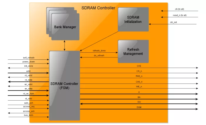
The SDRAM Controller implements a controller for Single Data Rate Synchronous Dynamic Random Access Memory (SDR SDRAM) devices as…
The SDRAM Controller implements a controller for Single Data Rate Synchronous Dynamic Random Access Memory (SDR SDRAM) devices as specified in the JEDEC Standard No. 21-C Page 3.11.5.1 Release 12.
Single Data Rate SDRAM can accept one command and transfer one word of data per clock cycle. Typical clock frequencies are 100 and 133 MHz. Chips are made with a variety of data bus sizes. SDRAM is still being manufactured and the maturity of this technology makes it ideal for systems that need performance at a low cost.
The SDRAM Controller has been developed to DAL A according to the DO-254 / ED-80 and is accompanied by a Certification Kit. For lower DAL levels reduced documentation sets are available. The core is also available as a netlist for DAL D or projects not needing the full RTL source.
Implementation Details
Unless otherwise specified (marked with an *) all the runs have been performed with the default options of the respective tool .
The following example implementations are compatible with two MT48LC4M16A2 memory chips in parallel (each SDRAM chips contains 64Mb with 4K rows, 4 banks, 256 columns and 16bits per word).
The results are provided for an SDRAM Controller with the following configuration generics (see Table 1):
| ‘g_DATA_WIDTH’ | 32 |
| ‘g_ROW_BITS’ | 12 |
| ‘g_COL_BITS’ | 8 |
| ‘g_BANK_BITS’ | 2 |
| ‘g_CAS_LATENCY’ | 2 |
| ‘g_BURST_TYPE’ | ‘0’ (Sequential) |
| ‘g_BURST_LENGTH’ | “011” (8) |
| ‘g_WR_BURST_MODE’ | ‘0’ (Programmed Burst Length) |
| ‘g_BUS_TURN_AROUND’ | 0 |
| ‘g_USE_ADVANCED_BST’ | See Note |
| ‘g_INIT_DELAY’ | 100000 (100 µs) |
| ‘g_INIT_REFRESH_NUM’ | 8 |
| ‘g_tREF’ | 64000000 (64 ms) |
| ‘g_tCK’ | 10 or 6 (ns) for 100 MHz and 166 MHz respectively |
| ‘g_tRP’ | 20 (ns) |
| ‘g_tRAS’ | 44 (ns) |
| ‘g_tRCD’ | 20 (ns) |
| ‘g_tRC’ | 66 (ns) |
| ‘g_tRRD’ | 15 (ns) |
| ‘g_tRFC’ | 66 (ns) |
| ‘g_tWRa’ | 18 (ns) |
| ‘g_tWRm’ | 15 (ns) |
| ‘g_tXSR’ | 67 (ns) |
| ‘g_tMRD’ | 2 (clock cycles) |
The following constraints were added:
In the tables below two results are shown for each device, the 1st one is with ‘g_USE_ADVANCED_BST’ set to TRUE and the second set to FALSE.
ALTERA
| FPGA Type | Maximum ‘clk’ Frequency | Flip-Flops | ALUTs | ALMs | Logic Cells |
|---|---|---|---|---|---|
| MAX II
(EPM2210F265C3) |
63.55 MHz
94.48 MHz |
267
267 |
–
– |
–
– |
929
739 |
| Cyclone III
(EP3C5F256C6) |
108 MHz*
156.2 MHz |
263
260 |
–
– |
–
– |
779
595 |
| Stratix II
(EP2S60F484C3) |
138.6 MHz
204.96 MHz |
264
261 |
547
353 |
402
267 |
–
– |
| Stratix III
(EP3SE110F780I3) |
166.69 MHz*
197.59 MHz |
279
261 |
525
347 |
433
279 |
–
– |
| Stratix IV
(EP4SGX70HF35I3) |
182.35 MHz
205.38 MHz |
262
263 |
529
343 |
411
300 |
–
– |
XILINX
| FPGA Type | Maximum ‘clk‘ Frequency | Flip-Flops | LUTs | Slices | Macrocells |
|---|---|---|---|---|---|
| Spartan3
(XC3S500E-5FG320) |
70.3 MHz
108.5 MHz |
262
261 |
871
580 |
572
364 |
–
– |
| Spartan6
(XC6SLX9-3FTG256) |
111.1 MHz
166.8 MHz |
271
268 |
754
540 |
273
159 |
–
– |
| Virtex4
(XC4VLX15-12SF363) |
134.5 MHz
169.6 MHz |
262
268 |
867
666 |
499
401 |
–
– |
| Virtex5
(XC5VLX30-3FF324) |
171.4 MHz
178.6 MHz |
261
265 |
–
– |
229
235 |
–
– |
| Kintex7
(XC7K70T-3FBG484) |
169.6 MHz
209.3 MHz |
246
241 |
700
417 |
242
148 |
–
– |
Note: some files may require an NDA depending on provider policy.

SDRAM Controller DO-254 IP Core is a DDR IP core from SafeCore Devices listed on Semi IP Hub.
Engineers should review the overview, key features, supported foundries and nodes, maturity, deliverables, and provider information before shortlisting this DDR IP.
Yes. Buyers can compare this product with similar semiconductor IP cores or IP families based on category, provider, process options, and structured technical specifications.