Vendor: Analog Bits Inc. Category: PLL

Core Powered FracN/SSCG PLL on TSMC CLN5

The Core Powered Fractional-N / Spread Spectrum PLL is an easy to integrate macro, requiring no analog power supply, and can be p…

Overview

The Core Powered Fractional-N / Spread Spectrum PLL is an easy to integrate macro, requiring no analog power supply, and can be placed anywhere on a chip.

This Fractional-N /Spread Spectrum PLL addresses power sensitive designs required for IOT, mobile and other low power applications needing non-integer clock multiplication, programmable clock synthesis, and clock tracking for fine tuning on-the-fly. The PLLs are designed for digitallogic processes and use robust design techniques to work in noisy SoC environments, such as high speed communication to low power consumer to memory interfaces.

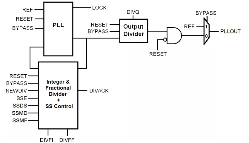
The programmable Fractional-N divider allows the PLL to lock to an incoming clock source and produce an output clock with a non-integer multiplication factor. The generated clock can be locked to the input source yet adjusted to a fine-degree of precision, and may be adjusted on-the-fly to maintain a relatively drifting local clock need. The updatable programmable fractional feedback divider is provided for this purpose. “On the fly” capability means the frequency transition and re-obtaining lock process for small frequency adjustment is glitch free and contains limited frequency over/undershoot.

Furthermore, itis a requirement by the FCC and equivalent international bodies that electronic devices including game-consoles, PCs, and high speed compute servers, limit Electromagnetic Interference (EMI) when they operate. The Spread Spectrum function of the PLL is capable of generating precise clock spreads (using a triangular modulation profile) that help reduce EMI. Programmable options allow the user to control the degree of spread in fine steps of modulation frequency and depth.

The PLL macro is implemented in Analog Bits’proprietary architecture that uses core and thick-oxide (1.2V and 1.2V-OD-1.5V) devices operated on a core voltage level power supply.

PLL Operational Range Description Symbol Min Typ Max Units Input Frequency FREF 5 600 MHz Post-Divide Reference Frequency (Integer mode) FPFD 5 200 MHz Post-Divide Reference Frequency (Frac/SS mode) FPFD 5 7.5 MHz VCO Frequency FVCO 8000 MHz Output Frequency FOUT 7.5 4000 MHz Output Duty Cycle tDO 45 55 % Area A 0.033 sq. mm Total Power IDD 16.7 mW Operational Voltage VDIG 0.675 0.75 0.825 V Operational Temperature TOP -40 25 125 C

Key features

  • Electrically Programmable PLL with Fractional-N divide and Spread Spectrum Clock Generation
  • Entirely core voltage powered, needs no analog supply voltage
  • Wide Ranges of Input and Output Frequency for diverse clocking needs
  • Very fine precision: near 1 part per billion resolution
  • Fully integrated 32-bit datapath (8-bit integer plus 24-bit fractional)
  • Ability to generate precise system clocks synchronized to track remote sources
  • Implemented with Analog Bits’ proprietary architecture
  • Low power consumption
  • Small area footprint
  • Excellent jitter performance with optimized noise rejection

Block Diagram

Silicon Options

Foundry Node Process Maturity
TSMC 5nm N5

Specifications

Identity

Part Number
Core Powered FracN/SSCG PLL on TSMC CLN5
Vendor
Analog Bits Inc.
Type
Silicon IP

Files

Note: some files may require an NDA depending on provider policy.

Provider

Learn more about PLL IP core

Creating a Frequency Plan for a System using a PLL

How do you ensure that every part of a system receives the clock it needs—without wasting power or sacrificing performance? The answer lies in creating a well-structured frequency plan built around a PLL.

Specifying a PLL Part 3: Jitter Budgeting for Synthesis

This white paper is aimed at system architects and physical implementation leaders working on the design of SoCs. It can be confusing to understand the impact of different jitter sources and how to calculate a jitter budget when specifying a digital system. This white paper explains how jitter changes the period of a clock and how to ensure that jitter has correctly been accounted for in the calculations for timing closure.

Specifying a PLL Part 2: Jitter Basics

This article explains a some of the key terminology and parameters commonly used to describe jitter. It will also help clarify the most important parameters for a some PLL applications, allowing the designer to better understand what is required from a PLL.

Specifying a PLL Part 1: Calculating PLL Clock Spur Requirements from ADC or DAC SFDR

In high end RF systems, such as 5G radios, the requirements are so stringent that the source of this strongest unwanted tone can be the PLL. This article outlines how spurs in the input clock to the ADC or DAC may limit the SFDR. This in turn will set the requirements for the spurs for the input clock (from a PLL), in order to achieve a specific SFDR.

Achieving Groundbreaking Performance with a Digital PLL

This article compares analog, first-generation digital, and second-generation digital PLLs. It evaluates which type of PLL may be best in which situation. It further discloses a roadmap into other application areas, including general purpose / logic clocking, and regular low-jitter PLLs.

Frequently asked questions about PLL IP cores

What is Core Powered FracN/SSCG PLL on TSMC CLN5?

Core Powered FracN/SSCG PLL on TSMC CLN5 is a PLL IP core from Analog Bits Inc. listed on Semi IP Hub. It is listed with support for tsmc.

How should engineers evaluate this PLL?

Engineers should review the overview, key features, supported foundries and nodes, maturity, deliverables, and provider information before shortlisting this PLL IP.

Can this semiconductor IP be compared with similar products?

Yes. Buyers can compare this product with similar semiconductor IP cores or IP families based on category, provider, process options, and structured technical specifications.

×
Semiconductor IP