32-Bit SPARC V8 Processor
The LEON4 processor builds on the success of its predecessors, providing enhanced performance and efficiency for demanding space …
Overview
The LEON4 processor builds on the success of its predecessors, providing enhanced performance and efficiency for demanding space and high-reliability applications.
The LEON4 is a synthesizable VHDL model of a 32-bit processor compliant with the SPARC V8 architecture. The model is highly configurable, and particularly suitable for system-on-chip (SOC) designs.
The LEON4 processor can be enhanced with fault-tolerance features against SEU errors. The processor can be efficiently implemented on FPGA and ASIC technologies and uses standard synchronous memory cells for cache and register file.
The LEON4 processor is fully parameterizable through the use of VHDL generics, and does not rely on any global configuration package. It is thus possible to instantiate several processor cores in the same design with different configurations.
Architecture
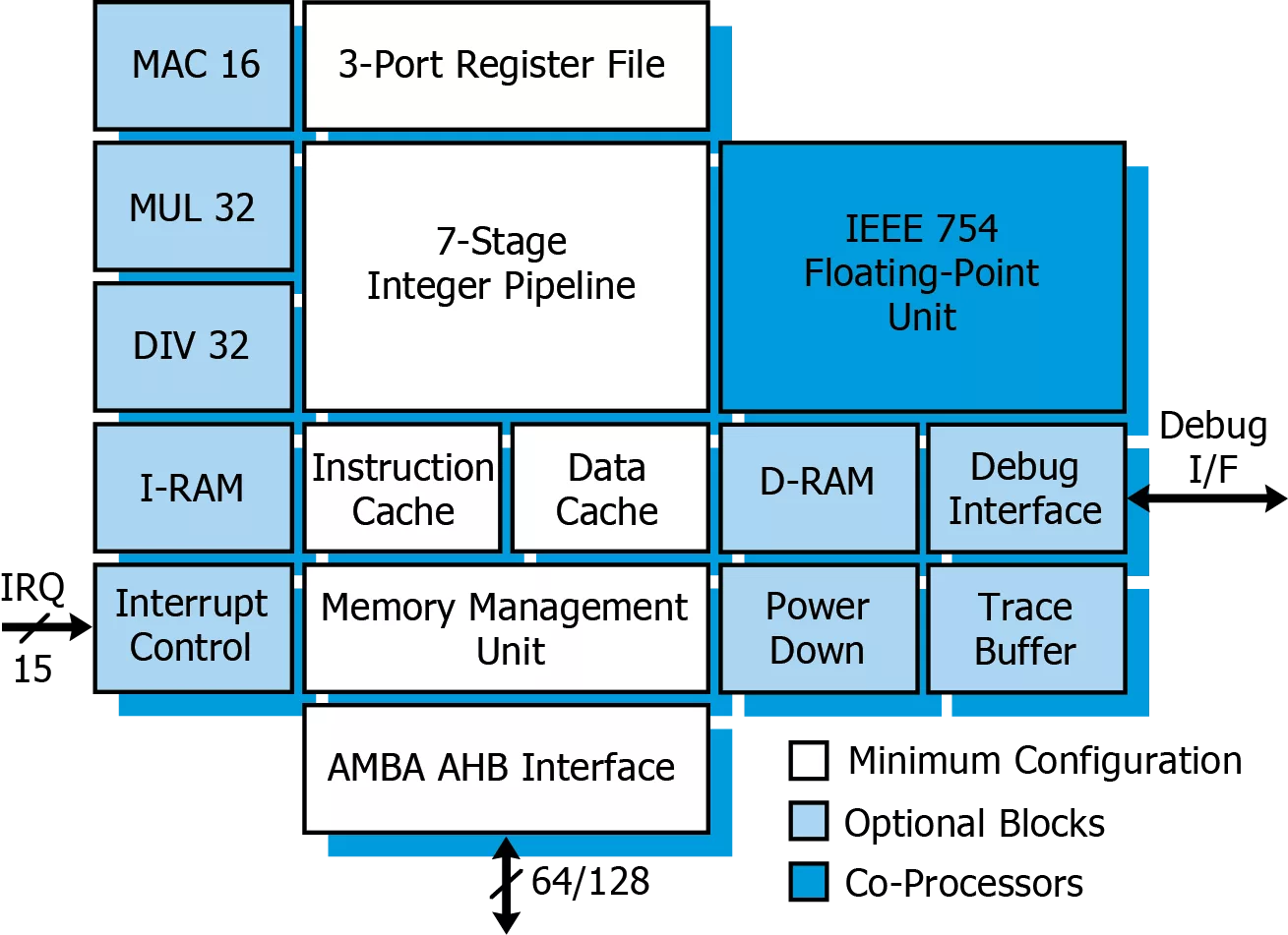
The LEON4 is interfaced using the AMBA 2.0 AHB bus and supports the IP core plug&play method provided in the GRLIB IP library. The processor supports the MUL, MAC and DIV instructions and an optional IEEE-754 floating-point unit (FPU) and Memory Management Unit (MMU).
The LEON4 cache system consists of separate I/D multi-set Level-1 (L1) caches with up to 4 ways per cache, and an optional Level-2 (L2) cache for increased performance in data-intensive applications.
The LEON4 pipeline uses 64-bit internal load/store data paths, with an AMBA AHB interface of either 64- or 128-bit. Branch prediction, 1-cycle load latency and a 32x32 multiplier results in a performance of 1.7 DMIPS/MHz, or 2.1 CoreMark/MHz.
Key features
- SPARC V8 instruction set with V8e extensions
- Advanced 7-stage pipeline, with branch prediction
- 64-bit single-clock load/store operation
- 64-bit 4-port register fileHardware multiply, divide and MAC units
- High-performance, fully pipelined IEEE-754 FPU
- Separate instruction and data L1 cache (Harvard architecture) with snooping
- Configurable caches L1: 1 - 4 ways, 1 - 256 kbytes/way. Random, LRR or LRU replacement
- Configurable L2 cache: 256-bit internal, 1-4 ways, 16 Kbyte - 8 Mbyte
- SPARC Reference MMU (SRMMU) with configurable TLB
- AMBA 2.0 AHB bus interface, 64- or 128-bit wide
- Advanced on-chip debug support with instruction and data trace buffer, and performance counter
- Symmetric Multi-processor support (SMP)
- Power-down mode and clock gatingRobust and fully synchronous single-edge clock design
- Up to 150 MHz in FPGA and 1500 MHz on 32 nm ASIC technologies
- Extensively configurable
- Large range of software tools: compilers, kernels, simulators and debug monitors
- High performance: 1.7 DMIPS/MHz, 2.1 CoreMark/MHz
Block Diagram
Specifications
Identity
Files
Note: some files may require an NDA depending on provider policy.
Provider
Learn more about CPU IP core
Announcing Arm AGI CPU: The silicon foundation for the agentic AI cloud era
ChiPy®: Bridge Neural Networks and C++ on Silicon — Full Inference Pipelines with Zero CPU Round-Trips
Unleashing Leading On-Device AI Performance and Efficiency with New Arm C1 CPU Cluster
Encarsia: Evaluating CPU Fuzzers via Automatic Bug Injection
Introducing Cortex-A320: Ultra-efficient Armv9 CPU Optimized for IoT
Frequently asked questions about CPU IP cores
What is 32-Bit SPARC V8 Processor?
32-Bit SPARC V8 Processor is a CPU IP core from Frontgrade Gaisler listed on Semi IP Hub.
How should engineers evaluate this CPU?
Engineers should review the overview, key features, supported foundries and nodes, maturity, deliverables, and provider information before shortlisting this CPU IP.
Can this semiconductor IP be compared with similar products?
Yes. Buyers can compare this product with similar semiconductor IP cores or IP families based on category, provider, process options, and structured technical specifications.