Overview
As the demand for higher data rates and increased serial I/O density intensifies, the performance requirements for next-generation SerDes designs become more stringent, particularly in managing area and power constraints. Multi-Gigabit/s serial transceivers are rapidly supplanted traditional parallel interfaces across numerous applications. High-speed transceivers must seamlessly support a range of data rates to accommodate new link speeds and emerging standards, all while maintaining backward compatibility with legacy systems. At elevated data rates, each component must meet rigorous performance specifications to ensure overall link integrity, especially in managing jitter and maintaining a strict bit error rate amidst challenging interconnect conditions such as channel loss, impedance discontinuities caused by packaging and connectors, and crosstalk from routing limitations in the package and motherboard.
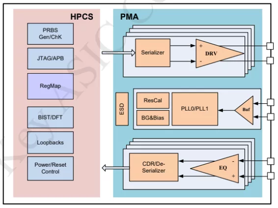
To effectively meet these challenges, serial I/O design has advanced, incorporating increasingly sophisticated architectures and cutting-edge techniques. Key ASIC’s multi-mode transceiver IP, which integrates both the PMA and PCS layers, is specifically engineered for applications demanding low power consumption and high performance. It is highly configurable and can be efficiently integrated with user logic or SoC resources, supporting data rates ranging from 1Gbps to 16Gbps.
Learn more about Multi-Protocol PHY IP core
As process nodes continue to shrink and core voltages drop to around 0.8V, the margin for noise in logic levels has become extremely small. Traditional RC-based reset circuits simply don’t have the precision needed to reliably tell the difference between a normal power-up sequence and a risky voltage fluctuation. That’s where Key ASIC’s Integrated Power-On Reset (POR) IP comes in.
Across the semiconductor industry, a great deal of attention is currently directed toward 112G SerDes and next-generation memory interfaces like DDR5. These developments are important to meet the growing demand for high-speed interfaces, but veteran SoC engineers who have taken over 100 designs into mass production often see the picture differently.
As we push beyond the 6.4 Gbps threshold with DDR5, the margin for error has essentially disappeared. For engineering leads and decision-makers, the goal is no longer just a simulation that looks functional. What we really need is First-Pass Silicon Success—a stable, high-yield product that works right from the very first tape-out.
This article outlines Key ASIC R&D team's upcoming PLL suitable for high-speed SerDes having ultra low jitter with LC- tank VCO, and supporting up to 16 GHz output clock to sample the data.
As factories, process plants, and robotics platforms become increasingly intelligent and interconnected, the demand for stable, low-latency data links has pushed Ethernet deeper into embedded systems. However, since designing Ethernet connectivity into industrial chips comes with its technical and logistical hurdles, engineers may face challenges when implementing Ethernet in industrial designs.
As PCIe 5.0 and 6.0 dominate headlines in the semiconductor industry, it’s tempting for every SoC design team to reach for the newest protocol available. But not every application needs blazing-fast 32GT/s throughput—and not every market segment can afford the power, complexity, and cost penalties that come with bleeding-edge PHYs.