Vendor: Cadence Design Systems, Inc. Category: Multi-Protocol PHY

10Gbps Multi-Link and Multi-Protocol PHY IP

Designed for multi-protocols running on single PHY macro and is compliant with USB 3.1, PCI Express (PCIe) 3.1, DisplayPort TX v1.4, Embedded DisplayPort TX v1.4b, SATA 3, QSGMII

PHY TSMC 5nm +3 FFC +2 Available on request View all specifications

Overview

SerDes requirements for system-on-chip (SoC) designs are becoming increasingly demanding and must support increasing numbers of protocols that must be optimized for cost-and power-sensitive mobile, wireless IoT, consumer, and automotive designs.

The Cadence 10Gbps multi-protocol PHY IP provides a flexible PHY IP that simplifies the design process without compromising performance, power, or silicon die area (PPA). The PHY IP is a lower-active and low-leakage power design crafted for mobile, wireless IoT, consumer, and automotive designs.

The PHY IP is designed for multi-protocols running on single PHY macro and is compliant with USB 3.1, PCI Express (PCIe) 3.1, DisplayPort TX v1.4, Embedded DisplayPort TX v1.4b, SATA 3, QSGMII, and SGMII specifications. The PCS complies with the PIPE 4.2 interfaces, and provides support for the dynamic equalization features of different protocols.

The PHY IP is architected to quickly and easily integrate into any SoC, and to connect seamlessly to Cadence or third-party PIPE-compliant controllers. It provides a cost-effective, versatile, and low-power solution for demanding applications. It offers SoC integrators the advanced capabilities, flexibility, and support that meet the requirements of high-performance designs.

The PHY IP is part of the comprehensive Cadence Design IP portfolio comprised of interface, memory, analog, and system and peripheral IP.

The PHY IP is a hard PHY macro available for TSMC processes. I/O pads and ESD structures are included. It is designed to easily integrate with a Cadence Controller IP for PCIe and USB, or any third-party controller with a PIPE-compliant interface. Raw SerDes interface is adopted for Ethernet and DisplayPort protocols.

PHY Architecture

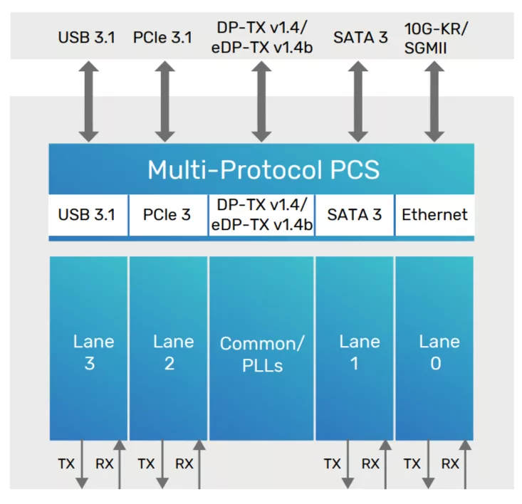
The PHY IP macro consists of a Physical Media Attachment (PMA) layer and a Physical Coding Sublayer (PCS). The Multi-Protocol and Multi-Link architecture PHY IP is highly configurable, allowing the PHY to be easily configured to your specific needs.

The PHY IP is designed with a lane-based architecture featuring one common support for up to eight lanes, providing greater control over floorplanning, placement, packaging, and I/O integration than other hard PHY solutions, while maintaining the reliability and ease of use associated with GDSII macros.

The PCS portion of the PHY provides the control, encoding, and protocol logic. The architecture partitions the PMA core into different primary sub-modules: common PLL, transmitter, and receiver lane modules. The PMA block provides the transmit, common PLL, and receive functions. The common PLL module also provides the interface between SCAN, Arm AMBA Bus, and JTAG and Analog Test including BIST, ABT, Scan, JTAG control, eye plotting, and PMA support logic functions.

Key features

  • Supports USB 3.1, PCIe 3.0/2.0/1.0, DP-TX v1.4/ eDP-TX v1.4b, SATA 3, QSGMII,and SGMII
  • Supports internal and external clock sources with clock active detection
  • Supports PCIe L1 sub-states
  • Automatic calibration of on-chip termination resistors 
  • Supports SRIS and internal SSC generation
  • Flexible lane configuration from 1 to 8 lanes
  • Multi-protocol support for simultaneous independent links
  • Scan, BIST, and serial/parallel loopback functions

Block Diagram

Benefits

  • Multi-protocol multi-link offers optimum SoC configurability
  • Optimized PPA for mobile and consumer applications
  • Extensive BIST and DFT enable ease of integration, faster bring-up, and quick debugging

What’s Included?

  • Standard integration views: LEF abstract, timing views (.LIB), behavioral model (Verily), gate-level netlist, SDF, DRC, LVS, ANT reports, and GDSII layout and layer map
  • Synthesizable soft PCS with SDC
  • Complete documentation including user guide, integration guide, and programmer guide
  • HVM kit
  • Testboards available upon request

Silicon Options

Foundry Node Process Maturity
TSMC 5nm N5 Available on request
TSMC 7nm N7 Available on request
TSMC 12nm FFC Available on request
TSMC 16nm FFC Available on request

Specifications

Identity

Part Number
10Gbps Multi-Link and Multi-Protocol PHY IP
Vendor
Cadence Design Systems, Inc.
Type
Silicon IP
Controller / PHY
PHY

Files

Note: some files may require an NDA depending on provider policy.

Provider

Learn more about Multi-Protocol PHY IP core

How a 16Gbps Multi-link, Multi-protocol SerDes PHY Can Transform Datacenter Connectivity

Increasingly, more of the focus on mobile has centered around cloud datacenters and the networking to get the data back and forth between these datacenters and the mobile device. Functions like voice recognition and mapping depend on the ability to split the functionality between the smartphone, for local processing like encryption and compression, and the back end, where a large number of servers can do the heavier lifting before returning the results.

One PHY, Zero Tradeoffs: Multi-Protocol PHY for Edge AI Interface Consolidation

The Cadence 10G multi-protocol PHY was architected to address this exact challenge. Designed to scale across multiple process nodes, it consolidates PCI Express (PCIe), USB, DisplayPort, Ethernet, and other interfaces into a single, compact, silicon-efficient block. What sets it apart is simultaneous multi-protocol support, which enables multiple data paths without duplicating hardware, requiring extra board connectors, or paying the area and power penalty of separate IP blocks.

Rethinking Edge AI Interconnects: Why Multi-Protocol Is the New Standard

Modern compute systems have evolved beyond reliance on a single dominant interface. Today, they're increasingly defined by their ability to support multiple high-speed protocols concurrently—including PCIe, Ethernet, and others. This shift toward multi-protocol capability is fundamentally reshaping how we architect intelligent edge AI systems, especially as inferencing workloads grow more distributed, data-intensive, and latency-sensitive.

Frequently asked questions about Multi-Protocol PHY IP cores

What is 10Gbps Multi-Link and Multi-Protocol PHY IP?

10Gbps Multi-Link and Multi-Protocol PHY IP is a Multi-Protocol PHY IP core from Cadence Design Systems, Inc. listed on Semi IP Hub. It is listed with support for tsmc Available on request.

How should engineers evaluate this Multi-Protocol PHY?

Engineers should review the overview, key features, supported foundries and nodes, maturity, deliverables, and provider information before shortlisting this Multi-Protocol PHY IP.

Can this semiconductor IP be compared with similar products?

Yes. Buyers can compare this product with similar semiconductor IP cores or IP families based on category, provider, process options, and structured technical specifications.

×
Semiconductor IP