Trusted Autonomy with Cadence Super Agents & NVIDIA Open Agent Safety Platform
Cadence AI Super Agents bring engineering trusted autonomy to semiconductor workflows, enabled by NVIDIA Open Agent Safety Platform.
10G-KR, XFI, PCIe 3.1/2.0/1.0, XAUI, QSGMII, SGMII, Gigabit Ethernet
Growing 10 Gigabit Ethernet deployments in the data centers and infotainment marketplace is driving the demand and connectivity needs of a broad range of high-end, energy efficient networking and computing applications.
Engineered for high-performance networking system and computing, the Cadence 10Gbps Multi-Protocol PHY IP supports multiple interface standards, including 10GBASE-KR, XFI, PCI Express (PCIe) 3.1, XAUI, QSGMII, SGMII, and 1G Ethernet for a flexible interconnect solution in system-on-chip (SoC) designs.
The PHY IP is designed to deliver high eye-margin at low power for backplane application. Numerous auto-calibrated circuits, programmable state machines throughout the design for PHY performance tuning, and the LC tank PLL provide a low-power optimum performance design. PCIe low-power states are also optimized to reduce total system power. All standard power states are supported.
The Cadence IP is engineered to quickly and easily integrate into any SoC, and to connect seamlessly with a Cadence or third-party PIPE 4.0-compliant controller. The IP is silicon-proven in multiple process nodes and has been extensively validated with multiple hardware platforms.
The Cadence 10Gbps Multi-Protocol PHY IP is part of the comprehensive Cadence Design IP portfolio comprised of interface, memory, analog, and system and peripheral IP.
The Cadence 10Gbps Multi-Protocol PHY IP is a hard PHY macro available for TSMC processes. I/O pads and ESD structures are included. It is designed to easily integrate with a Cadence Controller IP for PCIe or any third-party controller with a PIPE 3.1- or PIPE 4.0-compliant interface.
Architecture
The Cadence 10Gbps Multi-Protocol PHY IP macro consists of a physical media attachment (PMA) layer and a physical coding sublayer (PCS). Optimized for 10G Ethernet and PCIe 3.1 applications, the PHY IP provides long reach performances at low power with low area.
Compliant with IEEE Standard 802.3 10GBASE-KR requirements (Clause 51) and PCIe 3.1, 2.0, and 1.1, the Cadence 10Gbps Multi-Protocol PHY IP is highly configurable, allowing the PHY to be customized to your specific needs.
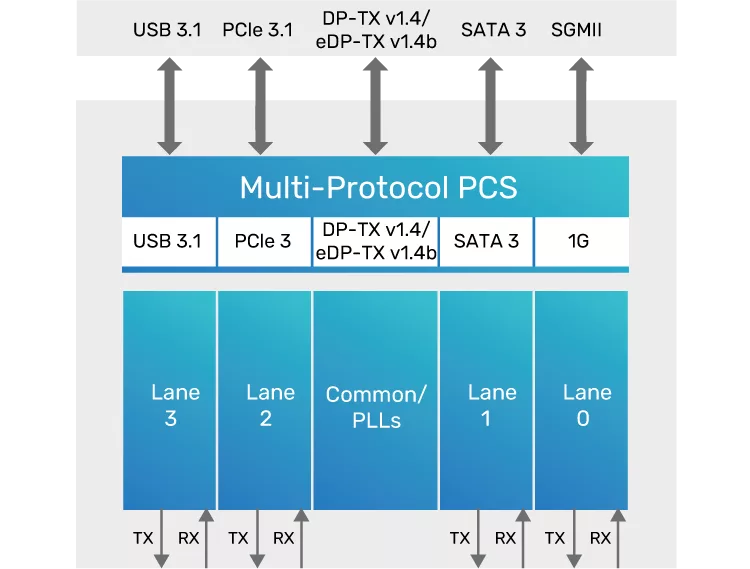
The Cadence 10Gbps Multi-Protocol PHY IP is designed with a lane-based architecture featuring one common support for up to 10 lanes, providing greater control over floorplanning, placement, packaging, and I/O integration than other hard PHY solutions, while maintaining the reliability and ease of use associated with GDSII macros. An on-chip PLL is compatible with selected reference frequency up to 156.25MHz with an available PLL lock status pin.
The PCS portion of the PHY provides the control, encoding, and protocol logic. The architecture partitions the PMA core into different primary sub-modules: common PLL, transmitter, and receiver lane modules. The PMA block provides the transmit, common PLL, and receive functions. The common PLL module provides the interface between Scan, Arm AMBA Bus, and JTAG and Analog Test including BIST, ABT/SAR, Scan, JTAG control, EYE plotting, and PMA support logic functions.
The transmitter module converts parallel data from the PCS interface to a serial data stream. The receiver module converts an input serial data stream to parallel data going to the PCS interface.
The Cadence 10Gbps Multi- Protocol PHY IP can be delivered in x1 to x16 configurations for PCIe, and 4x10G, 10x10G, and 1G for Ethernet. As an active member of many standards organizations, Cadence has early insight into emerging standards, and can quickly and easily adapt to critical and important changes to current standards.
| Foundry | Node | Process | Maturity |
|---|---|---|---|
| TSMC | 28nm | HPC | Available on request |
| TSMC | 28nm | HPC+ | Available on request |
| TSMC | 28nm | HPM | Available on request |
Note: some files may require an NDA depending on provider policy.

10Gbps Multi-Protocol PHY IP is a Multi-Protocol PHY IP core from Cadence Design Systems, Inc. listed on Semi IP Hub. It is listed with support for tsmc Available on request.
Engineers should review the overview, key features, supported foundries and nodes, maturity, deliverables, and provider information before shortlisting this Multi-Protocol PHY IP.
Yes. Buyers can compare this product with similar semiconductor IP cores or IP families based on category, provider, process options, and structured technical specifications.