Overview
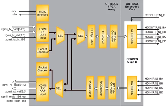
The 10 Gigabit Ethernet Extended Sublayer (XGXS) Intellectual Property (IP) Core enables the creation of system solutions for 10 Gigabit Ethernet (10 GbE) applications as defined by IEEE 802.3ae. This IP Core targets the pro-grammable array section of the ORCA ORT82G5 FPSC and provides a bridging function between 10 Gigabit Media Independent Interface (XGMII) and 10 Gigabit Attachment Unit Interface (XAUI) devices.
The ORT82G5 is a high-speed transceiver with an aggregate bandwidth of up to 29.6 Gbits/s that is targeted towards users in need of high-speed backplane and chip-to-chip interfaces using Ethernet and Fibre-Channel based protocols. The ORT82G5 has eight channels of integrated 0.6-3.7 Gbits/s SERDES channels that can be used as 2x10 Gbits/s XAUI interfaces.
XAUI is a high-speed interconnect that offers reduced pin count and is specified to drive up to 20 inches of PCB trace on standard FR-4 material. Each XAUI interface comprises four self-timed 8b/10b encoded serial lanes each operating at 3.125 Gbits/s and thus is capable of transferring data at an aggregate rate of 10 Gbits/s.
XGMII is a 156MHz Double Data Rate (DDR), parallel, short-reach interconnect interface (typically less than two inches). It supports interfacing to 10Gb/s Ethernet Media Access Control (MAC) and PHY devices.
In this design, the XGXS core is implemented in the FPGA portion of the device. A packet generator/checker and MDIO interface are also implemented in the FPGA logic.
The XGXS IP core is provided with implementation scripts, test benches, and documentation to allow users to integrate the functions for 10 GbE LAN/WAN applications.
Learn more about Single-Protocol PHY IP core
Combining Arm® AGI CPU server platforms with Lattice FPGAs and AMI firmware creates a solution that provides advanced security, manageability, connectivity, and flexibility for next-generation AI data center infrastructure.
Lattice Prompt pairs with AI agentic tools developers already use, combining them with Lattice design tools, knowledge base, and documentation to turn natural language inputs into validated responses, dramatically accelerating FPGA development while optimizing design performance and capability.
First announced on May 4, 2026, the acquisition creates the industry's most complete secure management and control platform.
The acquisition brings together Lattice’s industry-leading low power FPGAs with AMI’s industry‑leading platform firmware and infrastructure manageability solutions for cloud and AI to create a complete portfolio of secure management and control solutions.
The collaboration demonstrates a real-time AI sensor fusion architecture that integrates TI mmWave radar and camera sensors using NVIDIA Holoscan Sensor Bridge running on Lattice’s low power FPGA. The FPGA acts as a companion chip delivering synchronized sensor data directly into GPU-accessible memory to enable low-latency and robust perception for robotics and industrial edge AI applications.
Sets new standard for secure control FPGAs with full CNSA 2.0-compliant post-quantum cryptography, crypto-agility, and hardware Root of Trust for next-generation infrastructure