From Shrinking Transistors to Compressing Time: Deciphering Huawei’s τ Law
Huawei’s answer to Moore’s Law without EUV promises 14A performance by 2031.
By Echo Zhao, EE Times | May 26, 2026
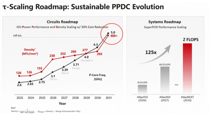
As Moore’s Law gradually becomes ineffective, the semiconductor industry seeks new paths to performance growth. At the 2026 IEEE ISCAS conference in Shanghai, Huawei said it has shifted performance optimization from “geometric size” to “time compression,” and validated this through engineering practice (using 381 chips designed and mass-produced over the past six years).
In her keynote speech at ISCAS 2026, He Tingbo, president of Huawei Semiconductor, began by saying, “Over the past six years, I’ve often been asked: How did you survive and return to the forefront in highly competitive industries such as smartphones and AI?”
To read the full article, click here
Related Semiconductor IP
- Mesochronous Bridge for PCIe/CXL
- AI-native GPU
- OpenGMSL Verification IP
- OpenGMSL Leaf IP
- FlexGen Multi-Die Smart Network-on-Chip (NoC) IP
Related News
- Necessity is the Mother of Invention: Huawei Replaces Moore’s Law With Her’s Law
- Huawei Files Lawsuit Against Motorola for IP Infringement
- TSMC Defends Transistor Scaling Amid Huawei’s ‘Her’s Law’ Proposal
- Nokia, Huawei sign W-CDMA patent licensing deal
Latest News
- SignatureIP Unveils MesoLink, a Mesochronous Bridge for PCIe/CXL Validation
- ICTK Partners with Jiran Security to Drive Post-Quantum Cryptography (PQC) Migration
- S2C Named Andes Technology’s 2026 Partner of the Year
- BrainChip Launches AKD1500 PCIe Card For Edge AI Evaluation Everywhere
- TDK-Micronas adopts Aniah’s AI-powered OneCheck® platform to advance automotive semiconductor development