Europe’s stealth leading-edge process technology
By Nick Flaherty, eeNews Europe | February 23, 2026
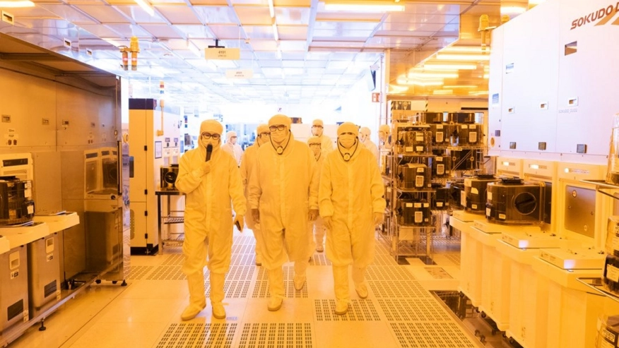
Europe has been at the forefront of semiconductor process technology for 40 years, but recently the calls to have leading edge technology in the region have grown louder.
For the last 20 years, a technology has been developed in the region that provides leading edge performance and can be manufactured in Europe. That technology is fully depleted silicon-on-insulator (FD-SOI), and the latest pilot line at CEA-Leti in Grenoble, France, promises to deliver the same performance as today’s 3nm technology, with lower cost and lower power consumption.
This process can be manufactured in Europe which is a critical step forward, not just for the automotive and industrial markets, but for chips for the exploding AI market where the region lags behind.
However the fact that FD-SOI can be a leading edge process for AI chips is perhaps not well known, as it has been focussed on analog mixed signal and radio devices.
To read the full article, click here
Related Semiconductor IP
- Ultra-low jitter, low-power ring-oscillator-based PLL-3GHz-4GHz
- Image Warping IP
- Image Warping IP
- ML-KEM-X Post-Quantum Cryptography Core
- AXI5 to/from AXI4 Bridge
Related News
- Perceptia Begins Port of pPLL03 to Samsung 14nm Process Technology
- Faraday Broadens IP Offerings on UMC’s 14nm Process for Edge AI and Consumer Markets
- Analog Bits Demonstrates Real-Time On-Chip Power Sensing and Delivery on TSMC N2P Process at TSMC 2026 Technology Symposiums
- M31 Collaborates with TSMC to Achieve Tapeout of eUSB2V2 on N2P Process, Advancing Design IP Ecosystem
Latest News
- Kandou AI Selects Baya Systems to Power Its Attack on the AI Memory Wall
- Arteris Expands Partnership with Arm to Accelerate Semiconductor Cybersecurity
- OpenTitan Earl Grey 2 to support CHERI and PQC
- TSMC June 2026 Revenue Report
- Quadric Extends Series C to $46M with Second Close led by World Bank's IFC