Why 28nm is the New Strategic Node?

If someone had predicted fifteen years ago that 28nm would still be the foundation for many new chip designs, the idea might have seemed unlikely. Process technology was advancing rapidly, and the industry’s attention was firmly fixed on shrinking geometries. Each new node promised more transistors, greater integration, and higher performance.
Yet, more than a decade later, 28nm continues to support new semiconductor products.
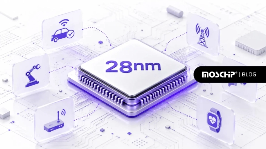 Rather than becoming another milestone on the technology roadmap, it has remained an active process node for applications spanning automotive electronics, industrial automation, networking, medical devices, consumer electronics, and edge computing. Its continued use reflects not only the characteristics of the process itself but also the evolution of priorities in semiconductor development.
This shift also reflects a broader change in how engineering teams evaluate process technologies. Choosing a node today is rarely a question of transistor density alone. Development teams also consider the design ecosystem, manufacturing readiness, IP availability, product lifespan, and the ability to move from architecture through turnkey ASIC development, manufacturing, and production with fewer unknowns. Viewed in that context, it becomes easier to understand why 28nm continues to occupy an important place in semiconductor development.
The evolution of 28nm
That role did not emerge overnight. When 28nm entered production, it offered the industry a practical combination of integration capability and design flexibility. As adoption grew, however, the process itself became only part of the story. The real change came from everything that developed around it.
Each generation of products added to the industry’s understanding of the node. Engineers refined floorplanning techniques, refined timing strategies, improved power optimization, and developed more predictable implementation flows. Foundries continued to optimize manufacturing, IP vendors expanded their portfolios, and EDA tools matured alongside real-world deployment.
That accumulated experience is often overlooked, but it matters. Designing on 28nm today is very different from designing on it a decade ago. Many of the questions that once required investigation have already been answered through years of production silicon. Engineering teams are able to build on established practices instead of developing new ones for every project.
In that sense, 28nm has evolved beyond a manufacturing technology. It has become a platform supported by years of practical engineering knowledge.
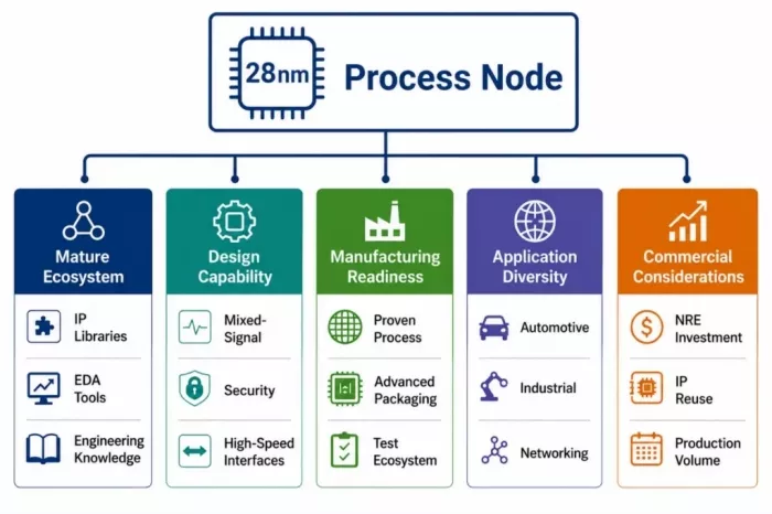
Key Characteristics of the 28nm Process Node
The 28nm ecosystem
That platform is especially visible in the ecosystem that now surrounds the node.
Over the years, 28nm has developed a well-established ecosystem with a broad portfolio of processor cores, memory compilers, interface IP, analog and mixed-signal building blocks, security modules, and standard cell libraries. Having been used across multiple product generations, these design resources provide engineers with technologies that are well understood and ready for integration into new designs.
The same applies to development flows. For most engineering teams, verification, timing closure, physical implementation, power analysis, and sign-off are familiar territory at 28nm. The focus is no longer on proving whether the methodology works, but on refining the product itself.
Another benefit is the amount of reusable engineering knowledge that now exists. Design reviews, implementation guidelines, verification strategies, and integration practices have all matured through repeated use. While every chip presents its own challenges, many of the supporting foundations are already in place, allowing development effort to be directed where it adds the greatest value.
Explore Analog & Mixed Signal IP
Manufacturing Advantages
By the time a process node has been in production for several years, the manufacturing ecosystem around it has also matured. Foundries have accumulated extensive production experience, process variations are better understood, and fabrication flows have been refined through successive production cycles.
For engineering teams, this means manufacturing is generally more predictable. Design qualification, silicon bring-up, and production planning can be carried out on a process that has already been used across a broad range of devices and manufacturing volumes. While every new design still requires careful validation, there is a well-established manufacturing foundation supporting that effort.
The same applies beyond wafer fabrication. Packaging, assembly, and test partners have worked with 28nm across multiple product generations, creating an ecosystem that supports products from prototype through volume production. For applications with long development cycles or extended market lifetimes, this continuity is often an important consideration.
Beyond technical considerations, process selection in product development is influenced by economic factors such as non-recurring engineering (NRE) investment, IP availability, and production volumes. The 28nm process node is evaluated alongside others based on technical and commercial considerations.
Supporting real-world applications
Taken together, these design and manufacturing advantages help explain why 28nm continues to appear in such a wide range of real-world products.
Automotive systems use it for applications ranging from infotainment and digital instrument clusters to gateway controllers and ADAS. Industrial equipment incorporates it in robotics, factory automation, motor control, and programmable logic controllers. Networking products continue to rely on it for switches, communication processors, and networking infrastructure.
Its presence extends well beyond those markets. Medical electronics, consumer devices, imaging systems, smart home products, and edge computing platforms continue to introduce new devices built on 28nm.
Although these products serve very different markets, they share one characteristic. They demand a process technology that supports integration, dependable manufacturing, and long product availability. The continued use of 28nm across such diverse applications reflects its ability to meet those requirements rather than any single technical advantage.
Design Capabilities at 28nm
This broad adoption is also supported by the capabilities the node offers to modern SoC designers. Today’s SoCs are expected to do far more than execute software. They combine processing, memory, connectivity, security, and analog functions within a single device, reducing board complexity while enabling increasingly sophisticated systems.
The 28nm process supports this level of integration across a broad range of applications. Embedded processors, on-chip memory, mixed-signal circuitry, hardware security, power management, and high-speed interfaces can all be integrated into the same design. Support for established standards such as USB, Ethernet, DDR, and MIPI further simplifies the development of connected systems.
The range of products developed on 28nm demonstrates its ability to support different system architectures and application requirements. This versatility is reflected in its continued use across multiple semiconductor markets.
Taken as a whole, the role of 28nm has changed considerably since it first entered production. What began as a new manufacturing node has grown into a technology platform backed by years of engineering experience, an established design ecosystem, and a manufacturing infrastructure that continues to support new semiconductor products, including ASIC design programs across a wide range of application domains.
Its continued use is not defined by when it was introduced or where it sits on the technology roadmap. Instead, it reflects the confidence that has been built around the node over years of practical deployment. As semiconductor products continue to diversify, 28nm remains an important part of that landscape, offering a combination of ecosystem maturity, manufacturing continuity, and design flexibility that continues to support new generations of silicon.
Organizations developing products often look for engineering partners that can support the complete silicon development lifecycle. In this area, MosChip Technologies works across the silicon design and development lifecycle, supporting programs from RTL to volume production. Its expertise includes turnkey ASIC execution, analog and mixed-signal design and layout, physical design, and IP integration, porting, and customization. MosChip supports designs across process nodes from 180nm to 2nm and is also a TSMC Design Center Alliance (DCA) partner.
FAQs
What is the difference between 28nm HPC, HPM, and LP process variants?
Foundries offer multiple 28nm variants optimized for high performance, low power, or balanced operation. Selecting the right variant depends on the application’s speed, power, and cost requirements.
Can an existing 40nm, 65nm, or 90nm ASIC be migrated to 28nm?
Yes. Many companies migrate legacy designs to 28nm to improve integration, reduce power, and add new functionality while preserving much of the existing architecture.
Is 28nm compatible with functional safety standards?
Yes. Many automotive and industrial products built on 28nm are designed to support safety standards such as ISO 26262 or IEC 61508, depending on the overall system design.
Is 28nm suitable for FPGA-to-ASIC migration?
Yes. Many FPGA-based products transition to 28nm ASICs to reduce unit cost, improve power efficiency, and optimize performance for volume production.
Related Semiconductor IP
- MIPI D-PHY Transmitter/Receiver for Samsung 28nm FD-SOI
- A 28nm 1.8V-3.3V Fail-Safe General-Purpose IO & OSC
- MIPI RX controller on SMIC 28nm
- 3.3V Capable GPIO on TSMC 28nm RF HPC+
- 1.2V Thin Oxide GPIO on TSMC 28nm RF HPC+
Related Blogs
- Rethinking Edge AI Interconnects: Why Multi-Protocol Is the New Standard
- Why What Where DIFI and the new version 1.3
- The Future of AI is Modular: Why the SiFive-NVIDIA Milestone Matters
- Power, Not Area: Why Edge GPU Design Is Entering a New Era