Simple Mode, Advanced Mode: A Clear Path to Closing Timing Around eFPGA

Most conversations about eFPGA and timing stop at reassurance: the fabric is hardened, the timing is characterized, trust the .lib file. That’s true, but it skips the question ASIC architects actually need answered when they sit down to close STA: how does the handoff work, and who owns which part of it? That’s the piece worth walking through.
Two modes, two jobs
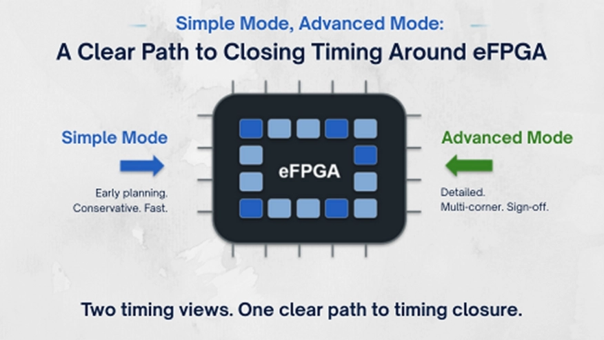 Hardened eFPGA IP is typically delivered with two distinct timing views and conflating them is where confusion usually starts.
Simple mode is a conservative, bounding-box timing model that captures worst-case delays across the eFPGA core’s interface, intended for early floorplanning, architectural what-if analysis, and initial constraint development. It lets an SoC design team run full-chip timing passes long before the fabric’s internal configuration is finalized, without waiting on a fully detailed model. It’s deliberately pessimistic: the goal is to avoid late surprises, not to squeeze out maximum performance early.
Advanced mode is the detailed, multi-corner timing view used for final sign-off. It reflects the characterized behavior of the fabric at the interface, across the full set of delivered process, voltage, and temperature corners, and is what the design closes against before tape-out.
Using simple mode where advanced mode belongs leaves margin on the table. Using advanced mode too early, before constraints have stabilized, just means redoing timing runs unnecessarily. Knowing which one your flow needs at each stage is most of what makes eFPGA timing closure straightforward rather than mysterious.
What “corners” actually cover
Timing corners are often where concerns about programmable logic really arise — the fear that a fabric’s behavior will drift unpredictably across operating conditions. Hardened eFPGA IP addresses this the same way any other hard macro does: the vendor delivers a defined corner set (process skew, voltage, temperature) with the timing collateral, and the SoC team applies its own margining on top, exactly as it would for any other block in the design.
QuickLogic delivers five corners with every hardened eFPGA IP core covering the process, voltage, and temperature combinations most programs need for full-chip timing closure and to maximize yield. For programs with wider environmental requirements or additional margin needs, we can extract and deliver additional corners on request — there’s no need to re-architect the fabric or redesign the flow.
For systems that need to operate across wider environmental ranges — extended temperature, radiation-tolerant processes, or other ruggedized requirements — that corner set can be extended accordingly, but the mechanism doesn’t change. You’re not inventing a new timing methodology for the fabric; you’re feeding it into the same corner-based margining discipline the rest of the chip already uses.
Who owns what?
This is the part that’s easy to get wrong if teams assume too much. In a hardened eFPGA integration, the division of responsibility looks like this:
- The IP provider owns characterizing the fabric itself — generating the timing models, defining the interface arcs, validating them against extracted layout or silicon, and delivering both simple and advanced views along with the supported corner set.
- The SoC team owns everything from the boundary outward — applying those models as constraints in their own STA environment, closing timing between the eFPGA interface and the rest of the chip, and handling any clock-domain crossings between the fabric and adjacent logic.
Neither side needs to reach into the other’s territory. The SoC team never needs visibility into the fabric’s internal routing to close chip-level timing, and the vendor’s model doesn’t need to anticipate every possible downstream use of the interface signals — just characterize them accurately.
There’s one more layer worth naming explicitly: timing within the fabric, for whatever logic gets mapped into it, is a separate step handled by QuickLogic’s Aurora FPGA user tool at configuration time — not part of chip-level STA at all. Keeping that distinction clear early avoids a common late-cycle confusion, where a team starts trying to close full-chip timing against internal fabric paths that were never meant to be part of that analysis.
Explore Quicklogic IP:
Why this matters more than it sounds like it should
None of this is exotic. It’s the same corner-based, boundary-driven methodology used for any hard macro. But because eFPGA carries the word “programmable” in its name, teams sometimes assume the timing story must be different — that closure will require some special new flow. It doesn’t. The two-mode delivery, the standard corner set, and the clean ownership split are exactly what let eFPGA timing closure fit into an existing STA methodology rather than requiring a new one.
Getting this handoff right early — knowing which timing view to pull at each design stage, and which corners actually apply to your program — is what turns “we’re not sure how eFPGA affects our schedule” into a non-question well before tape-out.
Related Semiconductor IP
Related Blogs
- Neuromorphic Computing: A Practical Path to Ultra-Efficient Edge Artificial Intelligence
- A Systematic Approach to Robust LVDS Integration in Advanced Node ASICs
- A design path to success exists for ultra-low-voltage SoCs
- Small Language Models: Efficient Arm Computing Enables a Custom AI Future