Radiation-Hardened by Design: Building Interfaces for Space and Nuclear on TSMC CMOS

Prepared by Emil Hågan and Wouter Faelens (Sofics), in collaboration with Magics Technologies. Presented at the 2025 TSMC OIP Forum.
 Most chips live an easy life with room temperature, clean power and a steady supply. The chips in this article do not. They sit inside nuclear reactors, ride on satellites and work next to particle beams, where a single stray particle can corrupt data or destroy a device.
In those places radiation is the enemy and standard electronics do not last. This talk is about how two Belgian companies solve that together. Magics Technologies designs radiation-hardened ICs, and Sofics designs the on-chip protection that keeps their interfaces alive. Both build on TSMC CMOS, so they get modern performance and supply while still surviving conditions that off-the-shelf parts cannot.
The world’s toughest environments
Radiation damages chips in two ways and both matter for a part that has to keep working for years in the field.
The first is total ionizing dose or TID. Ionizing radiation deposits charge that gets trapped in the gate and isolation oxides. That trapped charge shifts transistor threshold voltages and opens up leakage paths, so the circuit slowly drifts out of spec and eventually stops working. TID is cumulative, which means a part can pass every test on day one and still fail halfway through a mission.
The second is single event effects or SEE. Here a single high-energy particle strikes the silicon and dumps dense charge along its track in an instant. Depending on where it lands you get a soft error, such as a flipped memory bit or a hard one, such as latch-up that draws runaway current and destroys the device. Soft errors corrupt data and hard errors end the mission.
Nuclear plants, space, medical imaging and particle research all expose electronics to this. A normal commercial part is designed for a benign environment, with no margin for threshold drift and no defense against latch-up, so it is simply not built to survive.
A growing need for rad-hard electronics
Demand for radiation-hardened electronics keeps rising. Space exploration is accelerating, with missions to Mars, plans for a moon base and competition among private spaceflight companies. Aging nuclear plants from the 1960s and 70s are being decommissioned and some are now being recommissioned to power AI and data centers. Fusion research is expanding, and medical imaging keeps advancing. The market reflects all of it and the forecast in Figure 1. captures the trend.
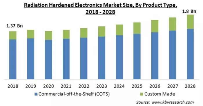
Figure 1: The radiation-hardened electronics market grows from about 1.37 billion USD in 2018 to 1.8 billion by 2028, split between commercial-off-the-shelf and custom-made parts. Source: KBV Research.
There are two ways to reach radiation hardness and the difference shapes everything downstream. Rad-hard by process uses a dedicated foundry flow where the silicon itself is made tolerant. It works, but those lines are expensive, low volume and usually a generation or two behind the mainstream. Rad-hard by design takes the opposite route, using a standard commercial process and solving the hardness in the circuit topology and layout instead. Magics takes the second path, which is what lets them build on TSMC and ride modern nodes, density and supply while still meeting the hardness targets.
Magics: rad-hard chips by design
Magics is based in Belgium with more than 10 years of leadership in this field, over 40 engineers and more than 10 ICs already in the market. Magics empowers pioneers in space and nuclear technology by providing critical electronics. They aim to be the world’s reference and go-to supplier for radiation-hard electronic products, for space, nuclear energy, and radiation-critical industries. They built that position partly through partnerships with local players such as Sofics. Their focus is highly reliable, high-performance ICs for the nuclear and space industries, delivered as several product families that can be tuned for a specific mission.
The numbers behind the hardness put it in context
Magics employs their radiation-hardening-by-design methodology in standard CMOS IC technologies to allow scalable solutions. Their parts withstand up to 100 Mrad of total ionizing dose, which is 1 MGy in silicon and roughly a thousand times what a typical commercial part tolerates. They also stay immune to single event effects up to an LET above 62.5 MeV·cm²/mg, well past normal industry levels. The catalog is organized as product series, shown in Figure 2.: Motion for moving parts and mechanisms, Time for precise timing, AI for processing, Power for management and Vision for imaging and video, alongside sensor interfaces.
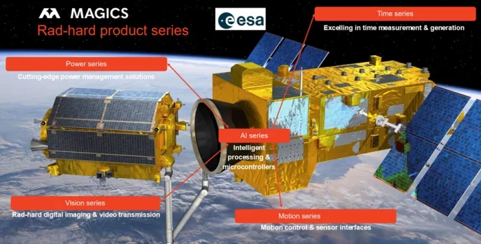
Figure 2: The Magics rad-hard product series. Motion for control and sensor interfaces, Time for measurement and generation, Power for management, AI for processing and microcontrollers, and Vision for digital imaging and video. Photo: ESA.
Fusion research shows why this matters. Magics contributes to ITER, the reactor in France built with research groups across Europe. It recreates the reaction that powers the Sun, a sustainable and non-carbon source that leaves far less radioactive waste than fission. But it needs remote maintenance and inspection, so cameras, sensors and control electronics sit near the reactor, where radiation passes 1 kGy and standard components cannot survive. Magics developed ICs that handle up to a thousand times that dose, beyond 1 MGy accumulated, and these hardened parts go directly into the fusion research systems.
The Time series is a concrete example, with a wideband PLL and frequency synthesizer.
- Output range: 1 MHz to 5 GHz
- Normalized phase noise: -223 dBc/Hz
- Phase noise: −120 dBc/Hz at 1 MHz offset, 5 GHz carrier
- TID: > 1 kGy
- SEL / SEU: > 62.5 MeV·cm²/mg, mitigated with triple modular redundancy
Each of these matters in orbit. Clean phase noise keeps high-speed serial links from losing data, and triple modular redundancy runs three copies of the logic that vote on every result, so a single upset is outvoted instead of propagating. That makes it suitable for on-board clock generation, serial links, jitter cleaning and switching supplies, all places where an unstable clock under particle radiation would be fatal.
Where Sofics fits: the interface problem
A rad-hard core is only half the job, because the chip still has to talk to the outside world and every pad needs ESD protection. On a Magics part that protection sits in the same radiation as everything else, so it has to clear the same bar as the core.
The clamps have to be rad-hard beyond 1 MGy, SEE-insensitive up to 80 MeV·cm²/mg and latch-up immune. At the same time they cannot slow the signal down or leak, which rules out simply making them bigger. And some interfaces are cold-spare (fail-safe), which adds a constraint most designers never meet. More on that below.
Standard foundry ESD libraries are not characterized for any of this, and that is the gap Sofics fills.
Cold-spare interfaces in space
Cold-spare is where this gets interesting, and it is a good example of a rule that only shows up in space.
High-energy particles can disrupt or damage a running chip, so many systems carry a backup, the spare circuit. That spare is usually left unpowered, hence cold, but it stays wired to the same communication lines as the active device. If the main device fails, the spare takes over.
The catch is what happens while it waits. The unpowered device still receives signals on its I/O, so the I/O voltage can sit higher than its own supply, which is at zero. A normal ESD network has a diode from the I/O pad up to VDD, but here that diode would conduct straight into the dead supply, loading the shared bus and leaking. So the usual diode up to VDD is not allowed. This is discussed in this article under full-local protection: Introduction: ESD protection concepts for I/Os.
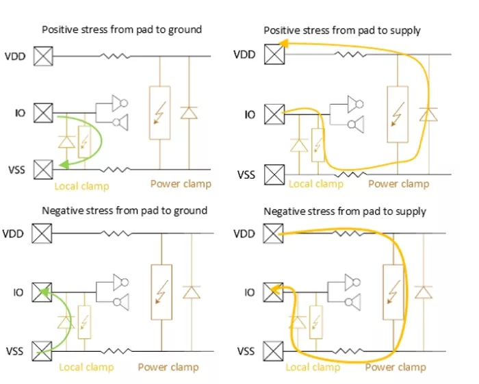
Figure 3: Positive ESD stress in a cold-spare interface. The semi-local clamp steers the discharge to ground through a local path. There is no diode up to the supply, so the unpowered device does not load the shared line.
Sofics solved this with a semi-local protection built specifically for cold-spare interfaces, shown for the two positive-stress cases in Figure 3. It gives ESD current a path to ground through a local device without ever referencing the dead supply rail, so the pin stays high-impedance to the bus while it is cold and still fully protected during a strike. The approach has been proven on for example TSMC 65nm.
- 1.2V interface: area < 1600 µm² | ESD > 2 kV HBM | leakage < 20 nA
- 3.3V interface: area < 1700 µm² | ESD > 2 kV HBM | leakage < 1 nA
The layouts for both cells are shown in Figure 4. Both sit between I/O and VSS, and the same idea has since been ported to mature and advanced nodes, which shows how well it scales across TSMC generations.
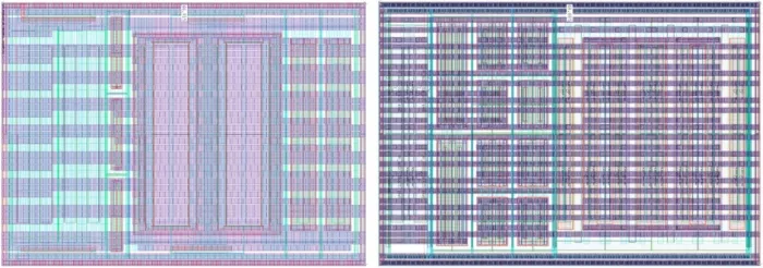
Figure 4: Cold-spare interface layouts on TSMC 65nm. The 1.2V cell on the left, the 3.3V cell on the right.
CERN and the 1.2V problem
CERN has worked with Sofics for over 10 years, on radiation-hard I/O and ESD without thick-oxide transistors. The cells are latch-up immune, low leakage and small area, with an over-voltage tolerant option and a low-capacitance local clamp for high-speed links. The libraries cover 1.2V and 0.9V on TSMC 65nm, 130nm and 28nm.
One request shows the pattern well. CERN needed a 1.2V I/O on TSMC 28nm. As always, Sofics first checked the standard TSMC GPIO library, which offered 0.9V on a thin-oxide core device and 1.8V or 2.5V on a thick-oxide IO device. There was no 1.2V option and CERN could not use thick-oxide transistors because they show worse total ionizing dose behavior and leak more under radiation over time.
So Sofics built a 1.2V GPIO entirely from thin-oxide 0.9V transistors. A single 0.9V device cannot safely hold 1.2V across its gate, so the design stacks devices in series to split the voltage, letting each one see only a safe fraction while the stack as a whole tolerates 1.2V. The result, shown in Figure 5. is a 1.2V interface with no thick oxide anywhere and full radiation hardness.
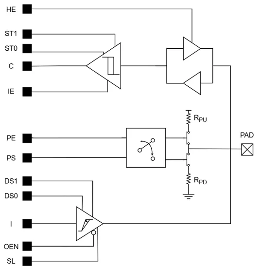
Figure 5: The 1.2V GPIO Sofics delivered for CERN on TSMC 28nm, built by stacking thin-gate 0.9V devices rather than using thick-oxide transistors.
Final takeaways
The message is simple. The world’s toughest environments need specialty circuits, because commercial parts do not survive there.
Magics builds radiation-hardened chips by design in standard CMOS for scalability.,Their products are tailored for the nuclear, space, aerospace and medical industries. Sofics provides the rad-hard on-chip ESD protection those chips need, proven on TSMC’s process platforms.
Sofics provides the rad-hard on-chip ESD protection those chips need, proven on TSMC’s process platforms.
Neither company does it alone. TSMC’s process platforms and Open Innovation Platform are what make the combination possible.
© 2025 Magics Technologies and Sofics.
More than 15 years with TSMC
Sofics has worked with TSMC for more than 15 years through the IP and DCA Alliance, with IP available on all TSMC process nodes. Sofics supports more than 90 TSMC customers, gets early access to the most advanced silicon and has its quality monitored by TSMC through the TSMC9000 program. At 2nm, TSMC named Sofics a primary vendor for GPIO and ESD. The recommendation runs both ways.
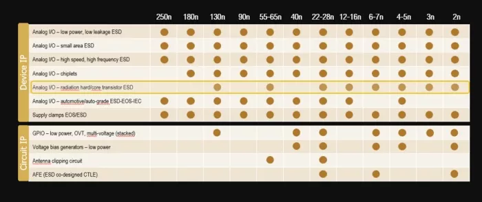
Figure 6: Sofics device and circuit IP spans from 250nm down to 2nm. Filled dots are in production, open dots are proven on silicon, squares are in simulation for the newest nodes.
Figure 6 reads by filled dots are already in production or on test-chip, for the newest nodes such as the 2nm nanosheet process, where Sofics recently received and measured its first parts. Behind that is a large track record: thousands of tape-outs, millions of wafers and billions of ICs across consumer, automotive, AI, medical, datacenter and space.
Some of those deployments are one of a kind. A Mars rover carries a customer’s radiation-hard FPGA that uses Sofics ESD protection, low in volume but unforgiving in its requirements. Others are satellite programs, CERN’s detectors and nuclear plant maintenance, all environments where the ESD cells have to survive the same radiation as the circuits they protect.
Related Semiconductor IP
- On-chip ESD/EOS/Latch up/EMC protection for high voltage and BCD processes
- Robust circuit and interface solutions
- On-chip ESD/EOS/Latch up protection for advanced and low voltage processes
- TSMC 40nm 5V GPIO
- TSMC 22nm 1.0V, 1.2V & 1.8V GPIO
Related Blogs
- Analog Bits Steals the Show with Working IP on TSMC 3nm and 2nm and a New Design Strategy
- Boost SoC Flexibility: 4 Design Tips for Memory Subsystems with Combo DDR3/4 Interfaces
- UA Link vs Interlaken: What you need to know about the right protocol for AI and HPC interconnect fabrics
- How Cadence and TSMC Are Accelerating AI Silicon Design at Advanced Nodes
Latest Blogs
- Mastering Semiconductor Chip Design: Tools, Techniques, and Best Practices
- Strategies for FPGA to ASIC Migration for Product Teams
- Two AI Brains Are Better Than One
- Your FPGA prototype runs. Can you see inside it?
- The Next Leap in Datacenter AI: Orchestrating Custom Accelerators with SiFive Intelligent Control Units (ACUs)