Protecting die-2-die interfaces...

There are several reasons to combine various chiplets in a single package, either next to each other (2.5D) or stacked on top of each other (3D) like the memory cube depicted below.
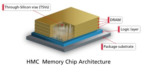
Example of a 3D stacked, co-packaged assembly. 4 layers of DRAM memory are stacked on top of a logic layer. Many of the interfaces between the logic layer and the memory devices stay within the package.
For instance, it enables chip designers to select the most optimal process for each type of function (interface, memory, compute, FPGA, analog circuits, MEMS, optical, …). It also allows to create chips with larger gate count when the reticle size is the limiting factor. And of course, yield improves a lot when the area of the die is reduced.
At Sofics we get a lot of questions about the required ESD robustness for the die-2-die (D2D) interfaces between chiplets in a package. People wonder how to select the right ESD standard (HBM, MM, CDM, TLP – more info) and what robustness level (1kV HBM?) they need to design for. Furthermore people wonder how they can validate the robustness once ESD devices are integrated?
What is the right ESD standard and ESD robustness level?
To read the full article, click here
Related Semiconductor IP
- Over-Voltage Lockout (OVLO) IP
- Verification IP for Universal Chiplet Interconnect Express (UCIe) up to 3.0
- UCIe-S (Gen2) Compatible PHY for Standard Package (x16) in TSMC N3P, North/South Orientation
- DSP-Based 112G SerDes
- XTAL oscillator in TSMC-7nm
Related Blogs
- SSD Interfaces and Performance Effects
- Protecting Against IP Theft
- On-chip interfaces gain importance in next-gen FPGAs
- Verifying MIPI interfaces in SoCs
Latest Blogs
- M31 High-Speed and Long-Channel MIPI C/D-PHY Solution on TSMC N3P/N3C
- Understanding security certification and how analog IP can help
- Embedded Security explained: Secure boot for embedded systems
- World's First Standards-Compliant 112G PHY IP for Linear Optics: A Turning Point for AI Interconnects
- One Key for Every Door: How Aliro Extends the UWB Digital Key Beyond the Car