CDM Dependence on Device Capacitance
This blog will focus on what happens during the CDM pulse itself, and will show how the pulse properties change as a function of DUT to Field Plate capacitance.
A TSMC 22nm Inline, Flip Chip compatible library with three-speed GPIOs and I2C compliant ODIO.
A TSMC 22nm Inline, Flip Chip compatible library with three-speed GPIOs and I2C compliant ODIO.
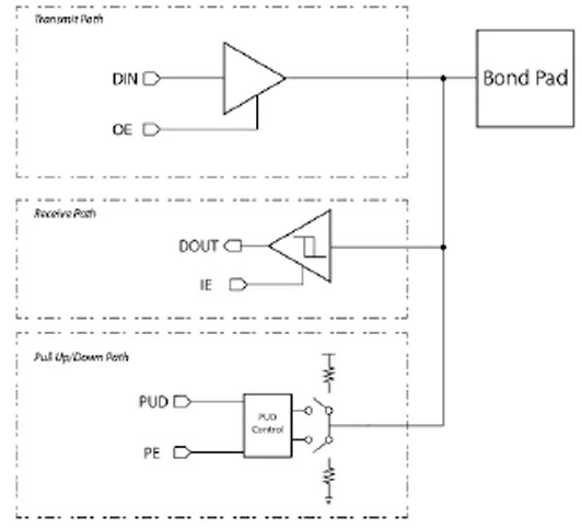
This silicon-proven, flip chip library in TSMC 22nm boasts three variants of GPIOs and one ODIO. All GPIO and ODIO cells have NS and EW orientation. All GPIO types are classified based on speed: 25MHz, 75MHz and 150MHz. All GPIO speed variants can operate at different post-driver voltage, which can be set at the system level and dynamically changed in the system if needed. The I/O includes a weak pull-up or pull-down resistor (approx. 60 Ohms). The ODIO is designed for lower speed interfaces but can be used as a high-voltage, high-speed input at up to 100MHz. The library is designed to allow for independent power sequences of any I/O cell, which is accomplished with an intrinsic power-on-control architecture. In the case of GPIO and ODIO, only when all powers are up and detected as ON, will the I/Os begin to function, otherwise they will remain in a high impedance state. Beyond standard ESD protection, the library is tolerant to 61000-4-2 IEC standard to 2kV.
Operating Conditions
| Parameter | Value |
| VDDIO | 1.8V or 3.3V |
| Core | 0.7V/0.8V/0.9V |
| Tj | -40C to 125C |
| ESD | >2kV HBM, 500V CDM |
Cell Size and Metal Stack
| Cell Size | Metal Stack |
| 30um x 130um | 1P9M_6X1Z1U |
Library Cell Summary
| Cell Type | Feature |
| Supply | 1.8V always on |
| IO150 | GPIO, operates at 150MHz (NS&EW) |
| IO75 | GPIO, operates at 75MHz (NS&EW) |
| IO25 | GPIO, operates at 25MHz (NS&EW) |
| ODIO | Open-Drain I/O (NS&EW) |
Standards
| Foundry | Node | Process | Maturity |
|---|---|---|---|
| TSMC | 22nm | ULL | — |
Note: some files may require an NDA depending on provider policy.

Three-Speed Inline Library with Open Drain I/0 in TSMC 22nm is a High-Speed IP core from Certus Semiconductor listed on Semi IP Hub. It is listed with support for tsmc.
Engineers should review the overview, key features, supported foundries and nodes, maturity, deliverables, and provider information before shortlisting this High-Speed IP.
Yes. Buyers can compare this product with similar semiconductor IP cores or IP families based on category, provider, process options, and structured technical specifications.