CDM Dependence on Device Capacitance
This blog will focus on what happens during the CDM pulse itself, and will show how the pulse properties change as a function of DUT to Field Plate capacitance.
A Specialized 1.2V to 3.3V Fail-Safe GPIO in Dongbu HiTek 110nm 11SB Pro- cess, with multiple protocol capabilties.
A Specialized 1.2V to 3.3V Fail-Safe GPIO in Dongbu HiTek 110nm 11SB Pro- cess, with multiple protocol capabilties.
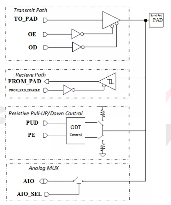
This silicon-proven Wirebond compatible library in Dongbu HiTek 110nm features a multi-voltage, multi-standard General Purpose Input Output with an Open-Drain Input Output capability, that targets the I2C standard. The library is built as a Fail- Safe I/O design. There is no poly-orientation for this library. The library features an Analog Mux, which allows for core direct access to the bondpad, either to drive externally a signal or receive a signal from the PAD. The I/O Library is compliant with standards regarding all 1.2V, 1.8V, and 3.3V operation. The library can support various standards, including I3C, I2C, SPI and QSPI. ESD targets are 2kV HMB and 500V CDM.
Operating Conditions
| Parameter | Value |
| Devices | 3.3V Thick & 1.2V Thin Oxides |
| BEOL | 1P7M |
| VDDIO | 1.2V, 1.8V or 3.V |
| VDD | 1.2V |
| Temp | -40C to 125C |
| ESD | 2kV HBM & 500V CDM |
| I/O Cell Size | 100x200um |
| Bondpad | 70x70um |
Cell Summary
| Foundry | Node | Process | Maturity |
|---|---|---|---|
| DB HiTek | 110nm | SB | — |
Note: some files may require an NDA depending on provider policy.

Multi-Standard Multi-Voltage Fail-Safe I/O in DB HiTek 110nm is a High-Speed IP core from Certus Semiconductor listed on Semi IP Hub. It is listed with support for dbhitek.
Engineers should review the overview, key features, supported foundries and nodes, maturity, deliverables, and provider information before shortlisting this High-Speed IP.
Yes. Buyers can compare this product with similar semiconductor IP cores or IP families based on category, provider, process options, and structured technical specifications.