Vendor: Cadence Design Systems, Inc. Category: HBM

Simulation VIP for HBM3

First to market with multiple early adopters of production designs.This Cadence® Verification IP (VIP) provides support for the H…

Verification IP Controller View all specifications

Overview

First to market with multiple early adopters of production designs.

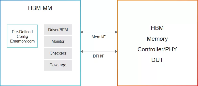
This Cadence® Verification IP (VIP) provides support for the High-Bandwidth Memory (HBM3) interface. It provides a highly capable compliance verification solution applicable to IP, system-on-chip (SoC), and system-level verification. The Cadence Memory Model for HBM3 models a single channel of HBM3 DRAM; this model can be replicated for multiple channels and stacks. The Memory Model for HBM3 runs on all leading simulators, and leverages the industry-standard Cadence Memory Model core architecture, interface, and use model.

The HBM3 DRAM standard is an industry-leading, low-power, double-data-rate, high-data-width, volatile (DRAM) device memory standard for storage of system code, software applications, and user data. The HBM3 DRAM Memory Device Standard is designed to satisfy the performance and memory density demands of the leading-edge high-performance devices.

Supported specification: JEDEC JESD235 Rev 1.27 (HBM), JESD235B Rev 2.50 (HBM2), JESD235B Rev 2.60 (HBM2E), latest HBM3 rev1.0 specification and newer revisions.

Key features

  • Speed (MHz)
    • Clock: 1800MHz; data rate: 7.2Gbps/pin
  • Mode Registers
    • All 16 mode registers are supported
  • Addressing
    • All addressing schemes with pseudo channels are supported
    • Device density from 2Gb to 32Gb per channel is supported
    • Device configuration from 8Gb, 8 High to 32Gb 16 High are supported
  • HBM3 Functionality
    • Precharge, Activate, Read, Write, Mode Register Set, Power Down, Self Refresh, and all related timing checks
  • Clocking and Reset
    • Differential clock inputs (CK_t/CK_c) and Active Low Reset Line (reset_n)
  • Initialization
    • Supports initialization with all tINIT* timing checks with options to skip initialization
  • Trainings
    • Supports WDQS-to-CK alignment training
  • DCA, DCM
    • Supports Duty Cycle Monitor and Duty Cycle Adjuster operations
  • Read/Write
    • Supports new WDQS-based architecture with 2X WDQS speed for Read and Write
    • Preamble and Postamble are supported
    • WDQS timing parameters and differential clocks are checked
    • tCCD related checkers are implemented
    • Supports unmatched WDQS to DQ path parameter - tWDQS2DQ
    • Supports auto-precharge feature
  • Refresh
    • Supports Refresh, Refresh Management, and Adaptive Refresh Management
  • SID
    • The stack ID (SID) acts as a bank address bit during command execution
  • Command Spacing
    • Command spacing checks
  • Bank Groups
    • Timing associated with back-to-back accesses to the same and different bank group
  • Command, Data Parity
    • Supports Command/Address parity, Data parity, and related checks
  • Data Bus Inversion (DBI)
    • Supports Write/ Read data inversion
  • IEEE 1500 Functionality
    • Supports all IEEE 1500 instructions decoding
    • Supports functionalities of instructions, likes of Mode Register Dump Set, HBM_RESET, Device ID, Channe Disable, etc
  • Loopback Test Mode
    • Supports all modes of AWORD and DWORD MISR operations
  • Boundary Scan
    • Supports Extest TX/RX instructions to test I/O connectivity
  • Redundancy Remapping
    • Supports Soft/Hard lane repair of AWORD, DWORD
  • WDQS Internal Oscillator
    • Supports WOSC operation using its IEEE instructions
  • ECC Engine Test Mode
    • Supports ECC engine test mode of operation
  • Temperature Compensated Refresh
    • Supports refresh rate information on TEMP pin, also supports sticky CATTRIP pin

Block Diagram

Specifications

Identity

Part Number
Simulation VIP for HBM3
Vendor
Cadence Design Systems, Inc.
Type
Verification IP
Controller / PHY
Controller

Files

Note: some files may require an NDA depending on provider policy.

Provider

Learn more about HBM IP core

High Bandwidth Memory Evolution from First Generation HBM to the Latest HBM4

HBM4 is the latest generation of the High Bandwidth Memory (HBM) that has become analogous to the Artificial Intelligence (AI) boom that is everywhere in today’s world. HBM is also increasingly being used in other applications like Data centers, autonomous driving systems, servers, cloud computing just to mention few domains where bandwidth and performance in a key requirement.

The Memory Imperative for Next-Generation AI Accelerator SoCs

AI accelerators are key components of the AI data center tasked with speeding up the complex mathematical calculations required for AI and machine learning (ML). As the demand for AI continues to skyrocket, it’s crucial that SoCs provide the necessary “brain power” for these AI accelerators to keep pace.

Heterogeneous Multicore using Cadence IP

This blog presents a heterogeneous multicore system built with the RISC-V Host CPU and Cadence IP: Xtensa DSPs, and the Janus Network-on-Chip (NoC). While this example uses an RISC-V CPU, any other ISA with similar capabilities can also serve as the host CPU.

Cadence Powers AI Infra Summit '25: Memory, Interconnect, and Interface Focus

AI is driving a new semiconductor renaissance—it's no longer just a workload, but the defining force behind a new era of semiconductor innovation. Cadence Fellow Charles Alpert echoed this message in his keynote, "Design for AI and AI for Design," offering insights into how AI is reshaping infrastructure and accelerating innovation.

Designing the AI Factories: Unlocking Innovation with Intelligent IP

The rapid evolution of artificial intelligence (AI) is reshaping the technological landscape, driving unprecedented demands on computing infrastructure. At the heart of this transformation lie innovations in intellectual property (IP) that enable scalable, efficient, and performance-driven AI factories.

HBM4 Boosts Memory Performance for AI Training

The recent HBM4 specification announced by JEDEC is great news for developers of AI training hardware. HBM4 is the latest specification in the rapidly evolving High Bandwidth Memory (HBM) DRAM standard, providing 2TB/s of memory performance and higher density up to 64GB (32Gb 16-high), according to JEDEC. "The advancements introduced by HBM4 are vital for applications that require efficient handling of large datasets and complex calculations, including generative artificial intelligence (AI), high-performance computing, high-end graphics cards, and servers," said the JEDEC release.

Frequently asked questions about HBM Interface IP

What is Simulation VIP for HBM3?

Simulation VIP for HBM3 is a HBM IP core from Cadence Design Systems, Inc. listed on Semi IP Hub.

How should engineers evaluate this HBM?

Engineers should review the overview, key features, supported foundries and nodes, maturity, deliverables, and provider information before shortlisting this HBM IP.

Can this semiconductor IP be compared with similar products?

Yes. Buyers can compare this product with similar semiconductor IP cores or IP families based on category, provider, process options, and structured technical specifications.

×
Semiconductor IP