
What is Parallel FLASH Memory Controller?
Parallel FLASH Memory Controller is a NOR Flash IP core from Zipcores Electronic Systems Engineering S.L. listed on Semi IP Hub.
FLASH_CONT is a JEDEC® compliant Flash controller IP Core that provides a convenient way of interfacing your FPGA or ASIC to an e…
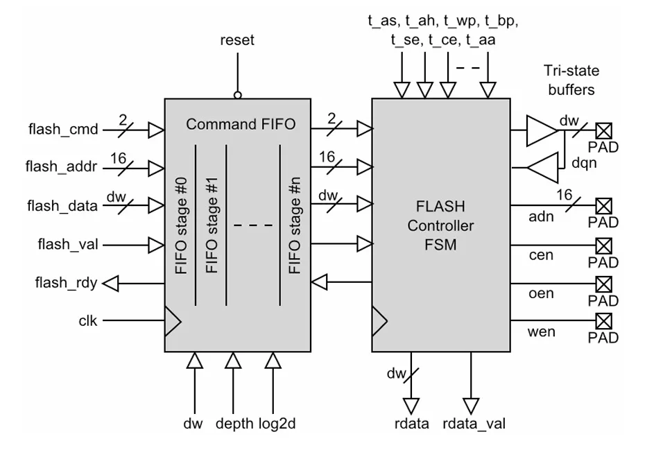
FLASH_CONT is a JEDEC® compliant Flash controller IP Core that provides a convenient way of interfacing your FPGA or ASIC to an external FLASH memory component. The IP Core features a simple-to use command interface and is fully synchronous with the system clock. The Flash controller is comprised of two main blocks. These blocks are the command FIFO and the main controller state machine that generates the correct signalling to the Flash memory.
The command FIFO uses the standard Zipcores valid-ready streaming protocol. This is a synchronous interface in which commands, addresses and data are written to the FIFO on the rising-edge of clk when flash_val and flash_rdy are both high1.
The command FIFO may be used to 'queue up' a sequence of commands to the Flash memory, and in doing so, can help to alleviate the speed differences between the system and the Flash device. The depth of the command FIFO may be configured with the generic parameters depth and log2d. Increasing the depth of the FIFO will allow more commands to be queued up. The 2-bit flash_cmd signal is decoded as follows:
The output ports to the Flash use a standard JEDEC pinout for an 8 or 16-bit EEPROM device. These pins may be connected directly to the external Flash memory component. The controller is compatible with most standard COTS devices such as those from Microchip®, Atmel®, AMD®, Winbond®, EON® and STmicroelectronics®.
Note: some files may require an NDA depending on provider policy.
Parallel FLASH Memory Controller is a NOR Flash IP core from Zipcores Electronic Systems Engineering S.L. listed on Semi IP Hub.
Engineers should review the overview, key features, supported foundries and nodes, maturity, deliverables, and provider information before shortlisting this NOR Flash IP.
Yes. Buyers can compare this product with similar semiconductor IP cores or IP families based on category, provider, process options, and structured technical specifications.