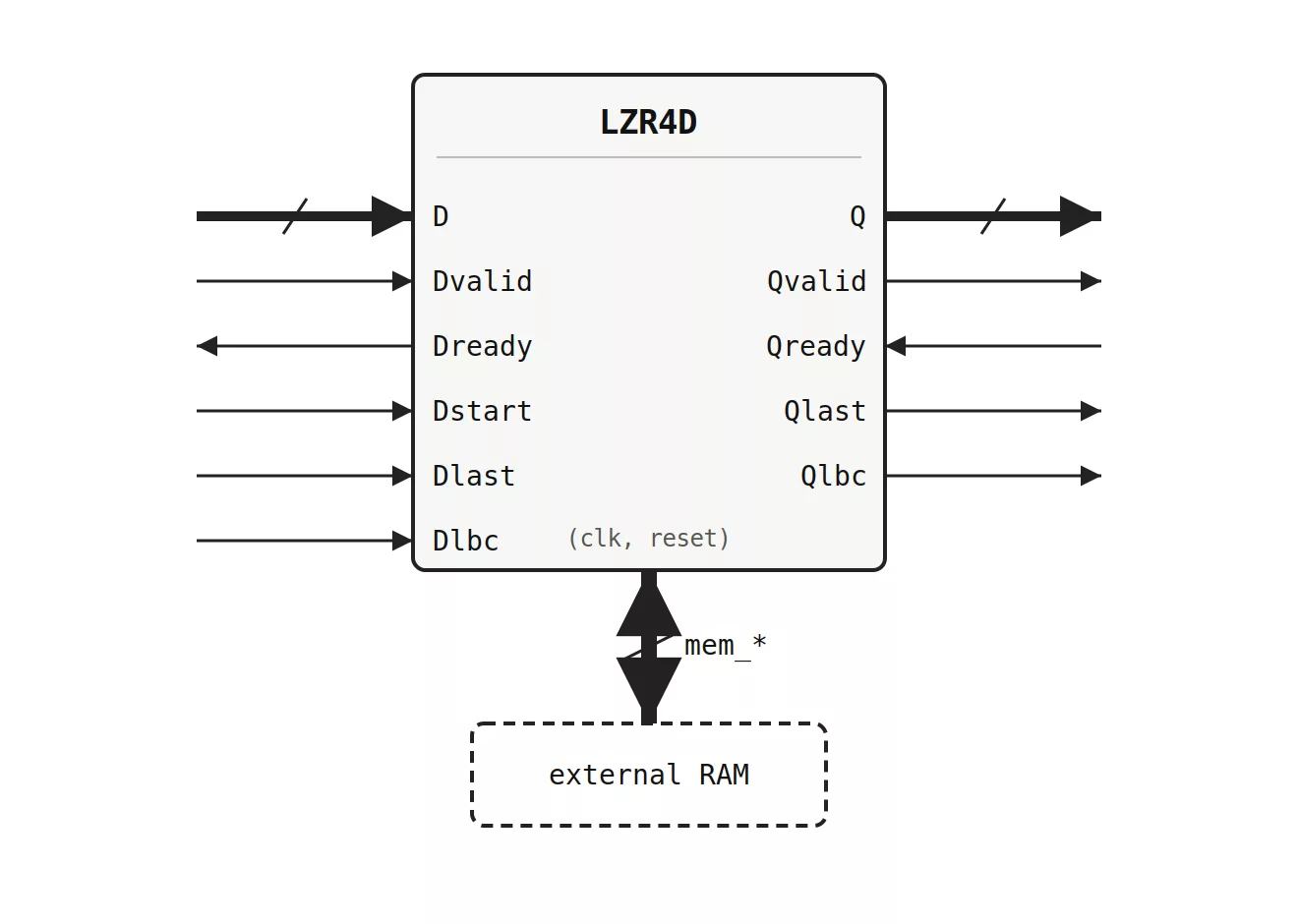
The LZR4D core implements lossless decompression of data compressed in the LZ4 format.
Unlike conventional few-bytes-per-clock or token-per-clock designs, the LZR4D resolves multiple LZ4 sequences concurrently within a single decompression engine, sustaining an output rate of 256 bits (32 bytes) of decompressed data per clock cycle on a single compressed stream. At the multi-gigahertz clock rates of advanced process nodes, this corresponds to terabit-class decompression throughput in a single engine, with no need to split data into independently compressed blocks across an array of slower decompressors
The core's decompression latency is below 30 clock cycles, which translates to an end-to-end decompression delay of 10 to 20 nanoseconds in advanced semiconductor nodes. This ultralow, deterministic latency allows the LZR4D to be placed directly in latency-critical data paths, such as compressed memory tiers, CXL-attached memory expanders, solid-state storage controllers, enterprise storage appliances, and in-network data processing, where the decompression step was previously a bottleneck.
Pin Description
| Name |
Type |
Description |
| CLK |
Input |
Core clock signal |
| RESET |
Input |
HIGH level synchronously resets the core |
| D |
Input |
Compressed input data bus, 8 bits width |
| Dvalid |
Input |
Data on D is valid |
| Dready |
Output |
Core is ready to accept data on D |
| Dstart |
Input |
Indicates the start of a new compressed frame on D |
| Dlast |
Input |
Indicates the last beat of the compressed frame on D |
| Dlbc |
Input |
Valid byte count in the last beat of D |
| Q |
Output |
Decompressed output data bus, 256 bits wide |
| Qvalid |
Output |
Data on Q is valid |
| Qready |
Input |
Indicates downstream is ready to accept data on Q |
| Qlast |
Output |
Indicates the last beat of the decompressed frame on Q |
| Qlbc |
Output |
Valid byte count in the last beat of Q |
| mem_* |
Bidirectional |
External RAM interface used by the decompression engine |