How Secure DDR Interfaces Protect DRAM from Memory Attacks
Brett Murdock, Dana Neustadter (Synopsys)
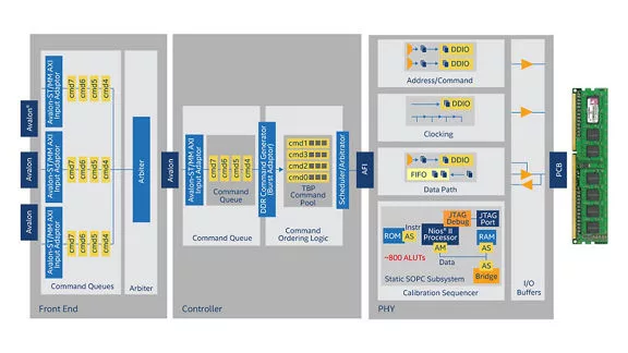
The High-Performance Memory Controller II SDRAM Intel FPGA IP core handles the complex aspects of using DDR, DDR2, and DDR3 SDRAM…
The High-Performance Memory Controller II SDRAM Intel FPGA IP core handles the complex aspects of using DDR, DDR2, and DDR3 SDRAM at speeds up to 933 MHz. The intellectual property (IP) core initializes the memory devices, manages SDRAM banks, translates read-and-write requests from the local interface into all the necessary SDRAM command signals, and performs command and data reordering.
The High-Performance Memory Controller II SDRAM Intel FPGA IP core is a drop-in replacement for the existing SDRAM controller with the following new enhanced features:
Note: some files may require an NDA depending on provider policy.
High-Performance Memory Controller II SDRAM Intel® FPGA IP Core is a DDR IP core from Altera listed on Semi IP Hub.
Engineers should review the overview, key features, supported foundries and nodes, maturity, deliverables, and provider information before shortlisting this DDR IP.
Yes. Buyers can compare this product with similar semiconductor IP cores or IP families based on category, provider, process options, and structured technical specifications.