Overview
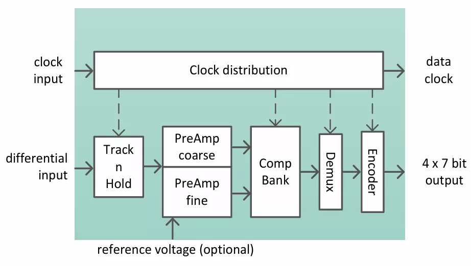
The IP consists of a 7 bit monolithic folding ADC clocked externally for 6 GS/s.
The differential input signal of maximum +/- 450 mV is ac-coupled to the input. Lower cut off frequency is well below 500 kHz.
The ADC is calibrated internally after reset to increase precision. The calibration can be disabled and can also be triggered manually.
The reference voltage is either derived from the 1.2 V supply or can alternatively be provided externally.
The IP needs an external clock with high accuracy and low jitter, because the clock jitter may influence the dynamic features of the converter. This clock is used as the sampling clock.
The digital output word of 7 bits is provided as a 4x parallel bus together with the clock.
The ADC is silicon evaluated in Fujitsu 55 nm CS250L technology.
Fraunhofer IIS provides a detailed documentation and support for the IP integration. Modifications, extensions and technology ports of the IP are available on request.
Learn more about ADC IP core
The Fraunhofer RISC-V Secure Element is now available as a licensable security platform for custom systems-on-chip (SoCs), application-specific integrated circuits (ASICs), and chiplets.
With the RISC-V Secure Element, the Fraunhofer Institutes for Integrated Circuits IIS, for Applied and Integrated Security AISEC, and for Electronic Microsystems and Solid State Technologies EMFT are introducing a security chip that was designed and manufactured in Germany.
For quite some time now, Fraunhofer IIS has been delivering MPEG-H Dialog +, a dialogue enhancement solution for broadcast and streaming. The codec separates speech from the rest of a film’s soundtrack and enables its separate enhancement.
The goal is to enable transport and storage of highest-quality image data in media and post-production workflows while maintaining full processing flexibility. This collaboration aims to significantly enhance the quality and performance as well as the time-cost-efficiency in current and future media production.
This forward-looking standard for professional video production pushes the boundaries of high-quality transmission over IP for a wide variety of applications in media and studio technology and streamlines real-time video processing in data centers.
The Fraunhofer Institute for Integrated Circuits IIS has developed an AI chip for processing spiking neural networks (SNNs). The inference accelerator for spiking neural networks SENNA is inspired by the functioning of the brain, consists of artificial neurons, and can process electrical impulses (spikes) directly. Its speed, energy efficiency, and compact design make it possible to use SNNs directly where the data is generated: in devices at the edge.