
Vendor: NTLab Category: ADC

2-bit 2-channel 100 MSPS flash ADC

The circuit is 2-bit ADC with programmable threshold.

2 Bit UMC 180nm BCD Silicon Proven View all specifications

Overview

The circuit is 2-bit ADC with programmable threshold. Least significant bit, calling sign bit, turns to 1 or 0 with changing of differential input signal polarity. Most significant bit, calling magnitude bit, turns to 1 if there is an excess of the threshold by differential input signal.
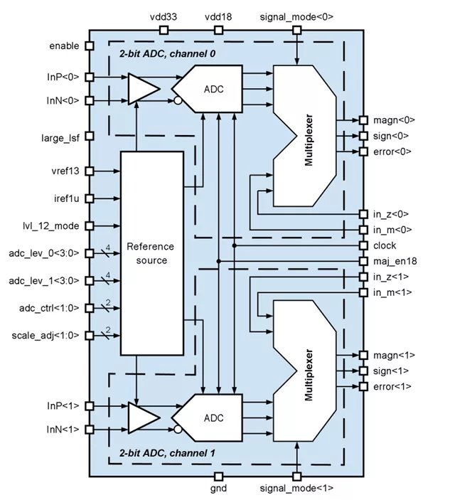
The block consists of reference voltages and currents generator, 2 voltage followers, 2 ADCs (for each channel) and multiplexers of input signal.
Thresholds are chosen by external 4-bit binary code in range from 60 mV to 220 mV. Threshold’s step equals 10 mV. There are two modes to define the threshold: «12 levels» mode and «16 levels» mode. Shifting between these modes is adjusted by logical level at lvl_12_mode input: logical “1” for «12 levels» mode; logical “0” for «16 levels» mode. There is a possibility to adjust the dc level of thresholds’ scale within 10 mV, wherein quantizing step remains unchangeable. Scale adjustment implemented by binary code at input scale_adj. Scale adjustment affects both channels at the same time.
There is logical error detector in ADC. In case of appearance one of faulty decisions logical level at the error output of corresponding channel. The faulty decisions are:
- Simultaneous signal of negative sign and upper threshold crossing
- Simultaneous signal of positive sign and lower threshold crossing
- Simultaneous signal of both upper and lower thresholds crossing
To avoid false operations there is the triple redundancy of comparators applied. The comparators are coupled by majority logic.

Key features

  • UMC CMOS 180 nm technology
  • Resolution 2 bit
  • Adjustment of threshold levels
  • Adjustment of dc level of thresholds scale
  • Analog supply voltage – 3.3 V; digital supply voltage – 1.8 V
  • Triple redundancy of comparators
  • Portable to other technologies (upon request)

Block Diagram

Applications

  • Correlators
  • Special processors in navigation systems
  • AGS systems

What’s Included?

  • Schematic or NetList
  • Abstract model (.lef and .lib files)
  • Layout view (optional)
  • Behavioral model (Verilog)
  • Extracted view (optional)
  • GDSII
  • DRC, LVS, antenna report
  • Test bench with saved configurations (optional)
  • Documentation

Silicon Options

Foundry Node Process Maturity
UMC 180nm BCD Silicon Proven

Specifications

Identity

Part Number
180UMC_ADC_01
Vendor
NTLab
Type
Silicon IP

Analog

Resolution bits
2 Bit

Files

Note: some files may require an NDA depending on provider policy.

Provider

HQ: Lithuania

Learn more about ADC IP core

Uncertainty-Guided Live Measurement Sequencing for Fast SAR ADC Linearity Testing

This paper introduces a novel closed-loop testing methodology for efficient linearity testing of high-resolution Successive Approximation Register (SAR) Analog-to-Digital Converters (ADCs). Existing test strategies, including histogram-based approaches, sine wave testing, and model-driven reconstruction, often rely on dense data acquisition followed by offline post-processing, which increases overall test time and complexity.

Three ways of looking at a sigma-delta ADC device

The growing availability of digital ICs like microcontrollers, microprocessors, and field-programmable gate arrays (FPGAs) allows developers to use complex digital processing techniques rather than analog signal conditioning. For this reason, analog-to-digital converters (ADCs) have become a widely-used component in mixed-signal circuits.

Specifying a PLL Part 1: Calculating PLL Clock Spur Requirements from ADC or DAC SFDR

In high end RF systems, such as 5G radios, the requirements are so stringent that the source of this strongest unwanted tone can be the PLL. This article outlines how spurs in the input clock to the ADC or DAC may limit the SFDR. This in turn will set the requirements for the spurs for the input clock (from a PLL), in order to achieve a specific SFDR.

Save power in IoT SoCs by leveraging ADC characteristics

Power-sensitive applications such as Internet-of-Things (IoT) require a comprehensive power savings strategy within the system-on-chip (SoC). Techniques relying solely on the use of traditional power down modes and low supply voltage may not be enough to achieve the required power targets. The analog block is often assumed to be too sensitive and not compatible with aggressive power management techniques.

High Speed ADC Data Transfer

When continuously running a high speed ADC, it can be a challenge to deal with the firehose of raw data available at the output. To use City Semiconductor’s 2.5 GS/s 12-bit ADC, for example, 30 gigabits per second of data have to be accepted.

Frequently asked questions about ADC IP cores

What is 2-bit 2-channel 100 MSPS flash ADC?

2-bit 2-channel 100 MSPS flash ADC is a ADC IP core from NTLab listed on Semi IP Hub. It is listed with support for umc Silicon Proven.

How should engineers evaluate this ADC?

Engineers should review the overview, key features, supported foundries and nodes, maturity, deliverables, and provider information before shortlisting this ADC IP.

Can this semiconductor IP be compared with similar products?

Yes. Buyers can compare this product with similar semiconductor IP cores or IP families based on category, provider, process options, and structured technical specifications.

×
Semiconductor IP