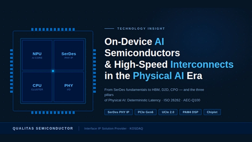
On-Device AI Semiconductors & High-speed Interconnects in the Physical AI era
On factory floors, robotic arms autonomously detect defective products. On the road, vehicles change lanes without a driver. AI is no longer confined to data centers. Physical AI — AI that has stepped into the physical world — is emerging as the defining theme in the semiconductor industry.
 If cloud AI is a "Super Brain" that thinks inside massive data centers, Physical AI is "Brain + Body." It senses the environment, makes instantaneous decisions, and acts — autonomous vehicles, collaborative robots, AMRs (Autonomous Mobile Robots), and drones all fall under this category. This is precisely why NVIDIA has declared "the next wave is Physical AI," and why leading semiconductor companies are aggressively advancing on-device AI semiconductor capabilities.
Physical AI has one fundamentally different requirement from cloud AI: mistakes are not tolerated. A 0.1-second delay in a cloud AI response is merely inconvenient, but a steering command delayed by a few milliseconds in an autonomous vehicle can cause an accident. This difference transforms the entire design philosophy of interconnects.
This post is based on a presentation by Jae-Young Kim, Executive Director (Ph.D.) of Qualitas Semiconductor, delivered at the Physical AI Frontier in March 2026. It provides an in-depth look at the fundamentals of high-speed interconnects, AI/HPC trends (HBM/D2D/CPO), and the three critical requirements of Physical AI: Deterministic Latency, Functional Safety (ISO 26262), and Automotive Reliability (AEC-Q100).
1. Overview of High-Speed Interconnects
1.1 What is Wireline Interconnect?
Wireline interconnect refers to the wired interfaces used in mobile devices, PCs, network servers, and more. Depending on the application, different standards are used, each optimized for specific bandwidth, distance, and power efficiency requirements.
- Die-to-Die: UCIe chiplets — connecting multiple dies within a single package
- On-board: PCIe, MIPI, eDP, V-by-1 — connecting components on a board
- Box-to-Box: USB, HDMI, DisplayPort, Ethernet — connecting devices
Looking at per-lane data rates for the latest wireline standards, there is a gap of more than 17x, from D-PHY at 6.5 Gb/s to Ethernet at 112 Gb/s. PCIe and Ethernet currently offer the highest transmission speeds.
1.2 SERDES (Serializer/Deserializer)
SERDES is a core IP block that serializes low-speed parallel data from within an SoC and transmits it over a single channel, then deserializes it back into parallel data on the receiving side.
- Serialize low-speed parallel data from SoC → transmit over single channel → deserialize
- Ultra-high-speed transmission per channel → further scalability with multiple channels
- Applied to most standards: USB, HDMI, DisplayPort, MIPI, PCIe, Ethernet, and more
SERDES removes loss, distortion, noise, reflection, and crosstalk from the channel, and recovers the clock and digital data.
1.3 Channel Equalization and Power Efficiency
When channel bandwidth (BW) is limited, ISI (Inter-Symbol Interference) occurs, causing pulses to spread in the time domain. The equalizer restores bandwidth in the frequency domain and removes pre/post-cursor ISI to reshape the pulse.
Greater channel loss leads to higher power consumption. Based on 100G/lane technology, the EPB (Energy per Bit) slope is approximately 0.35 pJ/bit/dB — for every 10 dB increase in insertion loss (IL), power consumption increases by 3.5 pJ/bit.
|
⚠ NOTE SERDES power consumption is not simply a chip-level issue. The vicious cycle of power consumption → heat generation → cooling → more power consumption translates into energy costs for the entire data center. In practice, approximately 50% of data center energy consumption is used for cooling. |
2. AI/HPC Era Technology Trends — HBM, D2D, CPO
2.1 The Explosive Computing Demand of AI/HPC
The growing scale of AI model parameters is driving an explosive increase in demand for computing resources. Computing requirements are growing 4–8x per year.
Take GPT-4 as an example: training a model with 100–180 billion parameters required approximately 25,000 NVIDIA A100 GPUs running for three months, with estimated training costs alone of around $63 million.
2.2 The Limits of SoC Performance and the End of Moore's Law
The formula "SoC (logic) performance ∝ number of integrated devices ∝ process scaling × die size" underpins Moore's Law, which predicted that transistor counts would double every 18 months. However, by the mid-2010s, the industry effectively declared Moore's Law broken.
The reticle size limit of advanced lithography processes acts as a physical wall:
-
EUV reticle: 26mm × 33mm = 858 mm²
-
High-NA EUV reticle: ~400 mm²
To overcome these physical constraints, the AI/HPC industry shifted to a chiplet architecture based on Die-to-Die (D2D) interfaces and multi-die packages. System-in-package based on chiplet architecture has become mainstream, driven by the explosive growth of AI computing power.
2.3 Interconnect Requirements for AI/HPC
AI infrastructure requires low power consumption (power efficiency) and minimal latency. The fundamental approach to reducing equalizers and FEC (Forward Error Correction) is to improve the channel itself. This demands interfaces with extremely short electrical channels and high edge bandwidth density.
| IO Type | Primary Use | Channel Distance | Speed/Lane | Power Efficiency |
| HBM | Processor–Memory | ~2mm (Interposer) | 9.2 Gbps (HBM3E) | ~1 pJ/bit |
| UCIe (D2D) | Processor–Processor | 2mm~25mm (pkg) | 32 Gbps | 0.5~1 pJ/bit |
| MIPI | Mobile/Sensor I/O | ~30cm (FPCB) | 9 Gbps (DPHY v3.0) | 1~2 pJ/bit |
| PCIe | System expansion/Storage | ~50cm (Main BD PCB) | 64→128 Gbps | 5~10 pJ/bit |
| Ethernet | Server node interconnect | ~10m (Rack-to-Rack) | 112→224 Gbps | 10~20 pJ/bit |
Figure 1 Key AI/HPC Interface Specification Comparison
2.4 HBM (High Bandwidth Memory)
HBM interconnect expands memory bus width from 64-bit to 1,024-bit to increase total bandwidth. It uses TSV (Through-Silicon Via) or Hybrid Bonding-based 3D traces between a DRAM memory stack and a logic die (acting as memory controller), combined with Si interposer-based 2.5D traces between the logic die and the processor.
Key specifications for the Si interposer channel include: trace pitch ~10 μm, trace width/space ~5 μm, RDL layer 2–4 levels, and length matching of 10–20 μm (skew control). With a total physical channel width of approximately 6 mm, the edge BW density reaches ~1.5 Tbps/mm.
| Version | Bus Width | Data Rate/Pin | BW/Stack | Representative System |
| HBM1 | 1024-bit | 1 Gbps | 128 GB/s | AMD Fury X |
| HBM2 | 1024-bit | 2.0 Gbps | 256 GB/s | NVIDIA P100 |
| HBM2E | 1024-bit | 3.2 Gbps | 410 GB/s | NVIDIA A100 |
| HBM3 | 1024-bit | 6.4 Gbps | 819 GB/s | NVIDIA H100 |
| HBM3E | 1024-bit | 9.2 Gbps | 1.2 TB/s | NVIDIA B200 |
| HBM4 | 2028-bit | 9.2 Gbps | 2.4 TB/s | NVIDIA Rubin (planned) |
Figure 2 HBM Generation-by-Generation Specification Comparison
2.5 Chiplet (D2D, UCIe)
Die-to-Die (D2D) interconnect connects chiplets within a single package, delivering low-latency, high-speed, high-density connectivity comparable to being on the same die. It supports universal connectivity for xPU-xPU or xPU-IO die combinations and multiple protocol adaptation.
UCIe (Universal Chiplet Interconnect Express) supports both Standard PKG and Advanced PKG formats. With Advanced PKG, it achieves edge BW density of 10.5 Tbps/mm and latency of ~2 ns.
2.6 CPO (Co-Packaged Optics)
CPO miniaturizes module-based Ethernet (or PCIe, UCIe) optical transceivers and integrates them directly into the package. Because the optical transceiver is placed right next to the processor, losses in the electrical channel are nearly eliminated. The key technology is Silicon Photonics integration, enabling extremely high-density optical transceiver implementation.
- Silicon Photonics: core technology for integrating optical transceivers
- Micro-Ring-based WDM (Wavelength Division Multiplexing): achieves high bandwidth density
|
💡 KEY INSIGHT NVIDIA's Spectrum-X Ethernet switch adopts the CPO approach, enabling 1.6 Tb/s transmission with just two external lasers. Compared to conventional pluggable (QSFP-DD) solutions that required eight lasers, this represents a 75% reduction in laser count. |
3. Physical AI — Real-Time Perception, Processing, and Actuation
3.1 What is Physical AI?
If cloud AI is the "Super Brain," Physical AI is "Brain + Body." The focus is shifting from AI training (Hyperscaler/HPC) to inference and immediate feedback (Edge).
- Robots and vehicles capable of sensing the physical environment and executing goal-directed actions
- Physical movement in the real world increases the risk of accidents
Representative Physical AI applications include autonomous vehicles, industrial collaborative robots (Xpeng, Rainbow Robotics), logistics AMRs (MiR), military robots (Boston Dynamics), and ADAS systems.
3.2 The Physical AI Data Path
The Physical AI data path consists of three stages: Perception → Processing → Actuation.
- Perception: Transmits data from dozens of sensors — cameras, radar, LiDAR, ultrasonic sensors, panel displays — without delay. MIPI (MIPI CSI-2/DSI) is the key interface.
- Processing: Utilizes enhanced processing capability through a chiplet connecting CPU, GPU, and NPU via D2D (UCIe). Memory is connected via HBM or LPDDR.
- Actuation: Reliably delivers control commands to actuators (motor controllers, ECUs) within a defined time window. PCIe is the key interface.
4. Three Critical Requirements for Physical AI Interconnects
In contrast to the high-bandwidth and peak-performance demands of AI scale-up/out, Physical AI prioritizes stable real-time operation. Three requirements must be met for real-time Perception–Processing–Actuation:
| Category | AI Scale-Up (Vertical) | AI Scale-Out (Horizontal) | Physical AI (Edge) |
| Core Goal | Maximize single-node performance | Scale cluster horizontally | Real-time Perception–Processing–Actuation |
| Key Interfaces | UCIe-A, NVLink, UALink, HBM | (Ultra-)Ethernet, InfiniBand | UCIe-S, PCIe, MIPI, LPDDR |
| Latency | Ultra-Low (ns) | Low (μs) | Deterministic (ms, worst-case guaranteed) |
| Reliability Requirements | ECC, thermal management | Congestion Control | ISO 26262 (ASIL), AEC-Q100 |
Figure 3 AI Scale-Up/Out vs. Physical AI Interconnect Comparison
4.1 Deterministic Latency
In Physical AI, delays in the "Input → Decision → Actuation" cycle can cause accidents, making worst-case latency management critical.
- Irregular interconnect latency (jitter) interferes with actuator timing and undermines system stability.
- The system must be designed to optimize FIFO synchronization and clock timing based on worst-case latency, while minimizing FEC computation delays.
4.2 Functional Safety — ISO 26262
ISO 26262 is an international functional safety standard aimed at ensuring the functional safety of automotive electronic systems. It mandates a systematic approach to monitoring and managing the entire lifecycle of HW/SW — from specification and development through production and operation.
The development process requires analysis of failure mechanisms and failure rates (FIT) based on the IP's operating model, and design verification of corresponding safety mechanisms.
ASIL (Automotive Safety Integrity Level) ratings are determined by the combination of S (Severity of harm) × E (Exposure probability) × C (Controllability).
|
Level |
Risk |
Safety Requirements |
Representative Use Case |
| QM | Lowest | General industrial quality (ISO 9001) | Audio, infotainment, simple convenience |
| ASIL A | Low | Basic diagnostics and fault checking | License plate lights, interior lighting |
| ASIL B | Moderate | SW verification and data integrity checks | Instrument cluster, rear sensors |
| ASIL C | High | Redundancy and robust error correction | Lane-keeping assist, cruise control |
| ASIL D | Highest | Zero-defect HW/SW verification | Brakes (ABS), steering (EPS), airbags |
Figure 4 ASIL Level Definitions and Representative Use Cases
4.3 Automotive Reliability — AEC-Q100
AEC-Q100 is the AEC (Automotive Electronics Council) reliability standard for automotive semiconductors. It defines stress test criteria to verify the probability of failure within the operational lifetime under harsh automotive environments.
IP design must account for Power & Thermal Integrity, ESD Protection, and NBTI/HCI margins.
|
AEC Grade |
Operating Temp. |
Temp. Cycling |
High-Temp Storage |
| Grade 0 | -40~150°C | TCH: -55~150°C, 2,000 cycles | 175°C: 1,000 hrs / 150°C: 2,000 hrs |
| Grade 1 | -40~125°C | TCH: -55~150°C, 1,000 cycles | 175°C: 500 hrs / 150°C: 1,000 hrs |
| Grade 2 | -40~105°C | TCB: -55~125°C, 1,000 cycles | 150°C: 1,000 hrs / 125°C: 1,000 hrs |
| Grade 3 | -40~85°C | TCB: -55~125°C, 1,000 cycles | 150°C: 1,000 hrs / 125°C: 1,000 hrs |
Figure 5 AEC-Q100 Grade Requirements
* NBTI: Negative Bias Temperature Instability — thermal defect in PMOS gate dielectric
* HCI: Hot Carrier Injection — channel carriers injected into gate dielectric, causing defects
5. IP Roadmap for Physical AI — Qualitas Semiconductor's Response
5.1 Interface IP Portfolio
Qualitas Semiconductor is pursuing ASIL-B/D and AEC-Q100 Grade 2 Ready certification for its MIPI, PCIe, and UCIe IP portfolios. The certification timeline is as follows:
- Q1 2025: FSM Process (ASIL-D) completed
- Q2 2026: IP (ASIL-B) certification completed
- Q4 2026: IP (ASIL-D) certification scheduled for completion
All IPs are designed in accordance with the AEC-Q100 Grade 2 standard. The key IP portfolio includes: D-PHY TX/RX PHY, C-PHY TX/RX PHY, SLVS-EC RX PHY, PCIe Gen4/Gen5/Gen6 PHY, USB SuperSpeed+ PHY, UCIe-S PHY, and UCIe-A PHY.
5.2 Total IP Solution — Market Positioning
Qualitas Semiconductor is one of the few IP providers capable of supplying PCIe Gen6, UCIe, and MIPI IP together as an integrated sub-system.
| IP | PCIe Gen6 (64 Gbps/lane) |
UCIe Standard/Advanced |
MIPI CSI-2/DSI-2/SLVS-EC |
| IP Ownership | ● | ● | ● |
| Controller | Partner | In-house | In-house |
| Sub-system Supply (PHY + Controller integrated) |
● | ● | ● |
Figure 6 Qualitas Semiconductor Key IP Portfolio
6. Conclusion and Summary
The AI semiconductor landscape is evolving simultaneously on two fronts. One is the AI/HPC front, pushing to process more computation faster within data centers. The other is the Physical AI front, where computation results must be immediately executed in the real world. Both fronts require high-speed interconnects, but what they demand is fundamentally different.
In the AI/HPC Scale-up/Scale-out domain, the core challenge for interconnects is bandwidth. HBM expands the memory bus from 64-bit to 1,024-bit to deliver terabyte-class bandwidth. D2D (UCIe) achieves chip-level latency for chiplet-to-chiplet connections. CPO brings optical transceivers into the package, revolutionizing power efficiency for rack-to-rack transmission. All these technologies share a single guiding principle: make channels as short as possible and bandwidth as wide as possible. High edge BW density based on advanced packaging and low-latency wideband transmission are key competitive variables in AI infrastructure.
In the Physical AI domain, the core challenge for interconnects lies in an entirely different place. A delayed steering command by a few milliseconds can cause an accident. An irregular control signal to a factory robot arm can stop production. In this world, worst-case latency guarantee — not average latency — becomes the design standard, and ISO 26262 (functional safety) and AEC-Q100 (automotive reliability) are mandatory requirements. Being fast is not enough. The system must be predictable, safe, and unwavering in extreme conditions.
Translating both demands into silicon is the role of interconnect IP. Following the Physical AI system data path, MIPI for Perception, UCIe and LPDDR for Processing, and PCIe for Actuation must all work in concert for a system to function as a whole. Remove any one interface and the chain breaks. The ability to supply MIPI, PCIe, UCIe, and LPDDR as an integrated sub-system is the true competitive edge in the Physical AI era.
Qualitas Semiconductor holds the critical interface IP portfolio and proven mass-production track record for the Physical AI era. With ASIL-B/D and AEC-Q100 Grade 2 certification for PCIe and UCIe underway, we are committed to designing the Physical AI era together — not through numbers on a spec sheet, but through silicon-proven reliability.
|
About the Author Jae-Young Kim, Executive Director, Ph.D. | Qualitas Semiconductor Co.,Ltd About Qualitas Semiconductor Qualitas Semiconductor is a leading interface IP solution provider, offering a comprehensive MIPI, PCIe, and UCIe IP portfolio for Physical AI system implementation. The company is progressing toward ASIL-B/D and AEC-Q100 Grade 2 certification, and is one of the few IP providers capable of supplying PCIe and UCIe IP as an integrated sub-system. Editor Helen Kim | MarCom | Qualitas Semiconductor Co.,Ltd |
Related Semiconductor IP
- Verification IP for C-PHY
- Band-Gap Voltage Reference with dual 2µA Current Source - X-FAB XT018
- 250nA-88μA Current Reference - X-FAB XT018-0.18μm BCD-on-SOI CMOS
- UCIe D2D Adapter & PHY Integrated IP
- Low Dropout (LDO) Regulator
Related Blogs
- Analog Design and Layout Migration automation in the AI era
- Physical AI at the Edge: A New Chapter in Device Intelligence
- Arm in the agentic era: Scaling the converged AI data center
- The Rise of Physical AI: When Intelligence Enters the Real World