Overview
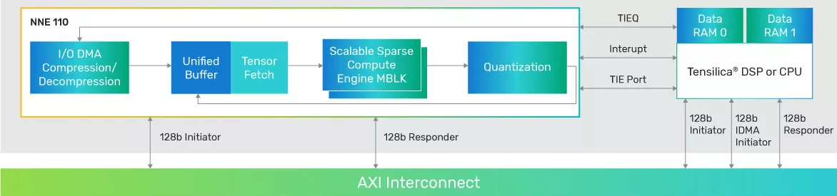
The Cadence® Tensilica® NNE 110 offers an energy-efficient hardware-based AI engine that can be paired with a Tensilica based DSP. The NNE 110 targets a variety of applications including audio, voice, and speech AI, lightweight vision AI, and always-on multi-sensory applications.
The product architecture natively supports the most common network layers found in these applications including convolution, depth-wise separable convolution, fully connected, LSTM, pooling, reshaping, and concatenation layers. Other layers can be supported (and further accelerated using TIE) using the host Tensilica DSP. The NNE 110 provides performance scalability from 32 to 128 MACs for 8x8-bit MAC computation, suiting a variety of low-power AI needs. It offers unique features for AI enhancement including hardware-based sparsity for compute and bandwidth reduction as well as on the-fly weight decompression for smaller system footprints.
Provider

Cadence Design Systems, Inc.
HQ:
USA
If you want to achieve silicon success, let Cadence help you choose the right IP solution and capture its full value in your SoC design. Cadence® IP solutions offer the combined advantages of a high-quality portfolio, an open platform, a modern IP factory approach to quality, and a strong ecosystem.
Now you can tackle IP-to-SoC development in a system context, focus your internal effort on differentiation, and leverage multi-function cores to do more, faster.
The Cadence IP Portfolio includes silicon-proven Tensilica® IP cores, analog PHY interfaces, standards-based IP cores, verification IP cores, and other solutions as well as customization services for current and emerging industry standards. The Cadence IP Factory provides you with an automated approach to the customization, delivery, and verification of SoC IP. As a result, you can spend more time on differentiation, with the assurance that you'll meet your performance, power, and area requirements.
Choosing Cadence IP enables you to design with confidence because you have more freedom to innovate your SoCs with less risk and faster time to market.
Learn more about Edge AI Accelerator IP core
While lightweight architectures like MobileNetV2 employ Depthwise Separable Convolutions (DSC) to reduce computational complexity, their multi-stage design introduces a critical performance bottleneck inherent to layer-by-layer execution: the high energy and latency cost of transferring intermediate feature maps to either large on-chip buffers or off-chip DRAM. To address this memory wall, this paper introduces a novel hardware accelerator architecture that utilizes a fused pixel-wise dataflow.
A look at Kinara’s accelerator and NXP processors which combine to deliver edge AI performance capable of delivering smart camera designs
In an ever-changing technology landscape, USB (Universal Serial Bus) has been a cornerstone since its inception in the mid-1990s. Initially designed to simplify the connection of peripherals to personal computers, USB has undergone significant transformations to meet the growing demands for faster data transfer rates, improved power delivery, and enhanced versatility.
Enter the Multi-Protocol SerDes (Serializer/Deserializer)—a flexible, reusable IP block that allows a single PHY to support multiple serial communication protocols, such as PCIe, SATA, Ethernet, USB, and more. This approach enables SoC vendors to meet diverse customer requirements and application needs without redesigning I/O for each target market.
Kurt Shuler, Arteris
William Ruby, Synopsys