Samsung Electronics and ASML expand strategic collaboration for next-generation semiconductor manufacturing
- Samsung joins industry initiative for 12-inch photomask platform for High NA EUV
- Samsung reinforces leadership with planned High NA EUV adoption for future DRAM manufacturing for the first time in the industry
SEOUL, Korea and VELDHOVEN, the Netherlands, September 8, 2026 -- Samsung Electronics and ASML today announced an expansion of their long-standing strategic partnership, deepening collaboration on High NA EUV lithography and advanced semiconductor manufacturing technologies that will help drive the next generation of innovation in the AI era.
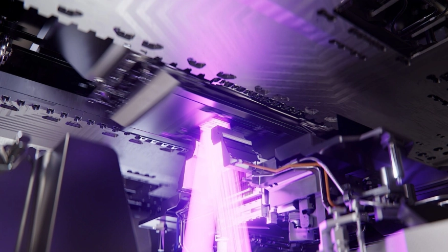 Building on years of successful cooperation, the companies will work together to accelerate the development and deployment of technologies that support the increasing performance and efficiency requirements of advanced semiconductor manufacturing.
Samsung will join the industry initiative to advance next-generation 12-inch photomask technology for future manufacturing. The semiconductor industry has relied on the 6-inch photomask format for decades. With High NA EUV, the transition to larger, 12-inch masks is expected to further increase fab productivity, lower chipmaking costs and remove stitching constraints. It will enable advanced chip manufacturers to fully leverage the advantages of High NA EUV, making future generations of leading-edge chips more cost-effective.
Drawing on its leadership in both memory and foundry manufacturing, as well as its extensive experience with advanced EUV lithography, Samsung is positioned to play a critical role in the 12-inch photomask transition. The company will work closely with industry partners to develop the required mask technologies and supporting infrastructure.
Samsung also plans to introduce ASML’s High NA extreme ultraviolet (EUV) lithography into future DRAM high-volume manufacturing for the first time in the industry by 2028, further demonstrating the readiness of High NA technology to support advanced memory and logic applications. High NA EUV is expected to extend the DRAM scaling roadmap, with improved resolution enabling process simplification and increased efficiency.
The announcement reflects a shared commitment to innovation, technology leadership and long-term partnership. Samsung and ASML expect to continue exploring opportunities for collaboration in areas including advanced memory and innovative manufacturing approaches.
Young Hyun Jun, Vice Chairman & CEO, Samsung Electronics said: "The AI era is transforming the semiconductor industry and increasing the importance of technological innovation across the entire value chain. Samsung is committed to maintaining leadership in advanced semiconductor manufacturing, including memory and foundry, through breakthrough technologies and strong partnerships. By further strengthening our collaboration with ASML, we are helping lay the foundation for the next generation of AI and semiconductor innovation."
Christophe Fouquet, President and Chief Executive Officer, ASML said: "Samsung has been one of ASML's most important innovation partners for many years. Together, we have helped advance the technologies that underpin modern semiconductor manufacturing. As the industry enters a new era driven by artificial intelligence, close collaboration with our customers becomes even more important. We look forward to working with Samsung to enable the next wave of semiconductor innovation."
Related Semiconductor IP
- MIPI D-PHY Transmitter/Receiver for Samsung 28nm FD-SOI
- 1.8V Capable GPIO on Samsung Foundry 4nm FinFET
- Temperature Sensor on Samsung 4nm, LN04LPP
- Temperature Sensor on Samsung 14nm, LN14LPP
- PVT Sensor on Samsung 4nm, LN04LPP
Related News
- Samsung Begins Chip Production Using 3nm Process Technology With GAA Architecture
- Samsung Electronics Unveils Plans for 1.4nm Process Technology and Investment for Production Capacity at Samsung Foundry Forum 2022
- Rambus and Samsung Electronics Extend Comprehensive Agreement
- Samsung Electronics' World-Class 5nm Technology Selected by Ambarella for New Automotive AI Central Domain Controller
Latest News
- JEDEC® Publishes First Industry-Wide Silicon Photonics Reliability Standard for AI, Datacenter and Telecom Infrastructure
- Orthogone Technologies Launches Ultra-Low-Latency FPGA IP Portfolio for Multi-Industry Deterministic Networking
- TIER IV joins Arm Total Design for Physical AI to accelerate ready-to-use Autoware solutions through Open AD Kit
- SEMIFIVE Signs Turnkey Contract with Mobilint to Develop Robotics AI Chip Under 'K-On-Device AI Semiconductor' Program
- ICTK to Acquire Network Security Firm withnetworks, Expanding from Security Chips into Global Enterprise Security Solutions