Nanoveu Gets First 16nm ECS-DoT Silicon from TSMC
A major technical milestone for the Company: engineering samples of EMASS’s next-generation ultra-low-power edge AI chip have arrived from the foundry, and benchmarking and characterisation now begin
- First engineering samples of the 16nm ECS-DoT system-on-chip (SoC) have been fabricated at TSMC and delivered to EMASS, Nanoveu’s wholly owned semiconductor subsidiary. The design now exists as physical silicon.
- A major technical milestone for the Company: The 16nm program has progressed through GDS sign-off (December 2025), tape-out and entry into fabrication at TSMC (January 2026) and now to packaged engineering samples, with each stage delivered as announced.
- 16nm joins 22nm: The 16nm ECS-DoT is built on TSMC’s 16nm FinFET process and sits alongside the commercially available 22nm ECS-DoT, giving EMASS a two-node product family running a common software toolchain and programming model.
- The chip carries every enhancement set out at tape-out: a fully integrated Bluetooth Low Energy subsystem with on-chip analog and RF, expanded on-chip SRAM, a new fine grained power-management fabric, a dedicated object-detection accelerator now protected by US Patent No. 12,651,452 B2, and the first hardware floating-point unit in the ECS-DoT family.
- Bring-up, benchmarking and characterisation to commence: The program will measure power, performance and functional behaviour across representative edge AI workloads, and the Company intends to publish a summary of measured results when it is complete.
- Smaller nodes remain on the roadmap: The Company continues to evaluate more advanced process nodes for future ECS-DoT generations.
September 22, 2026 -- Nanoveu Limited (“Nanoveu” or the “Company”) (ASX: NVU, OTCQB: NNVUF), a technology company specialising in advanced semiconductor, visualisation and materials sciences, is pleased to advise that its wholly owned subsidiary, Embedded A.I. Systems Pte. Ltd (“EMASS”), has received the first engineering samples of its next-generation 16nm ECS-DoT edge AI system-on-chip (“SoC”) from Taiwan Semiconductor Manufacturing Company (“TSMC”). The design that was signed off in December 2025 and taped out in January 2026 has now been manufactured on TSMC’s 16nm FinFET process and is in the hands of the EMASS engineering team. Receipt of first silicon is a major technical milestone for the Company and the first time an ECS-DoT device has been produced at an advanced FinFET node.
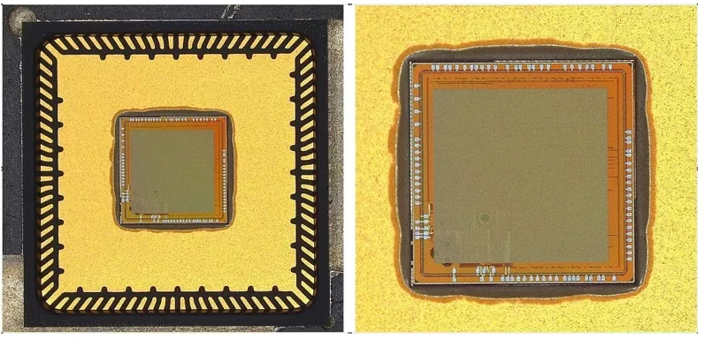
Figure 1: Packaged 16nm ECS-DoT engineering sample received from TSMC, with the die shown in detail at right.
From Tape-Out to Silicon
Receipt of first silicon is the point at which a chip program stops being a design and becomes a product. Everything before it, from architecture and RTL through synthesis, physical design and GDS sign-off, is work on a description of the chip. What EMASS holds today is the chip itself.
The 16nm ECS-DoT program reached this point in sequence. Front-end design, synthesis and physical design were completed and the design entered final GDS sign-off in December 2025. Tape-out followed in January 2026, when the mask data was released to TSMC and wafer fabrication began. The wafers have since been processed, diced and assembled into packaged engineering samples, which have now been delivered to EMASS.
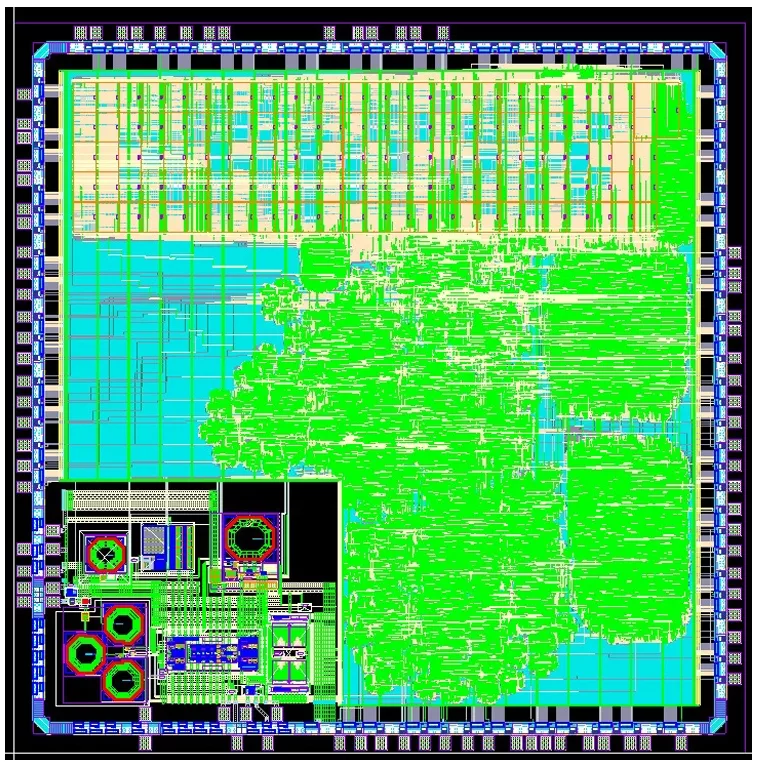
Figure 2: Physical layout of the 16nm ECS-DoT
16nm FinFET is an advanced node for ultra-low-power edge AI silicon. Moving to FinFET brings higher logic density, lower leakage and more headroom for on-chip integration, which is what allowed EMASS to place a full radio, a larger memory array and additional accelerators on the same die while holding to the power budget the ECS-DoT family was designed around.
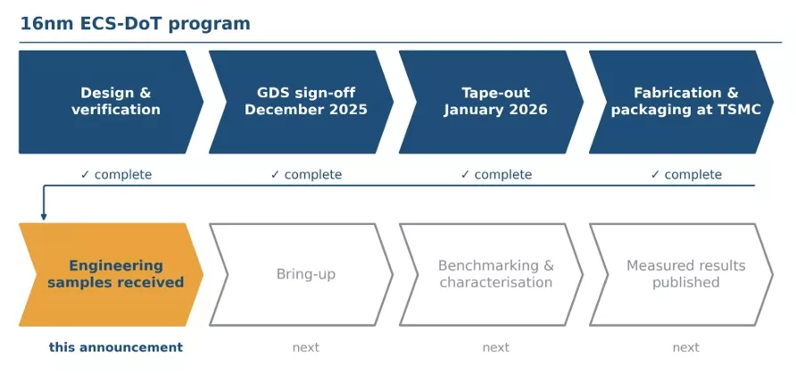
Figure 3: Status of the 16nm ECS-DoT program. Design, GDS sign-off, tape-out and fabrication are complete; bring-up, benchmarking and characterisation follow receipt of engineering samples.
Two Nodes, One Platform
EMASS now has ECS-DoT silicon at two process nodes, and the two devices are intended to do different, yet overlapping jobs.
The 22nm ECS-DoT is the Company’s commercial product and the device customers can design with today. It is in customer evaluation and design-in across wearables, industrial sensing, asset tracking, smart infrastructure and other always-on applications, including the asset tracking reference design with Bosch Sensortec announced in July 2026.
The 16nm ECS-DoT is the more fully integrated member of the family. It is aimed at customers who need more on-chip memory, who want to run vision alongside audio and sensor workloads, or who want the Bluetooth radio inside the SoC rather than as a separate part on the board. Both devices share one programming model, software stack and toolchain, so a customer can start on 22nm today and move to 16nm later with minimal changes to application code, and EMASS can support both from a single engineering base.
This is the position an established semiconductor company works from: a commercial device winning design-ins while the next generation is characterised behind it. It is the first time EMASS has held both at once.
What Is on the 16nm Chip
The 16nm ECS-DoT retains the RISC-V core, dual deep-learning accelerators, scalable compute-to-memory interconnect and always-on design philosophy of the 22nm generation and adds the following (Figure 4):
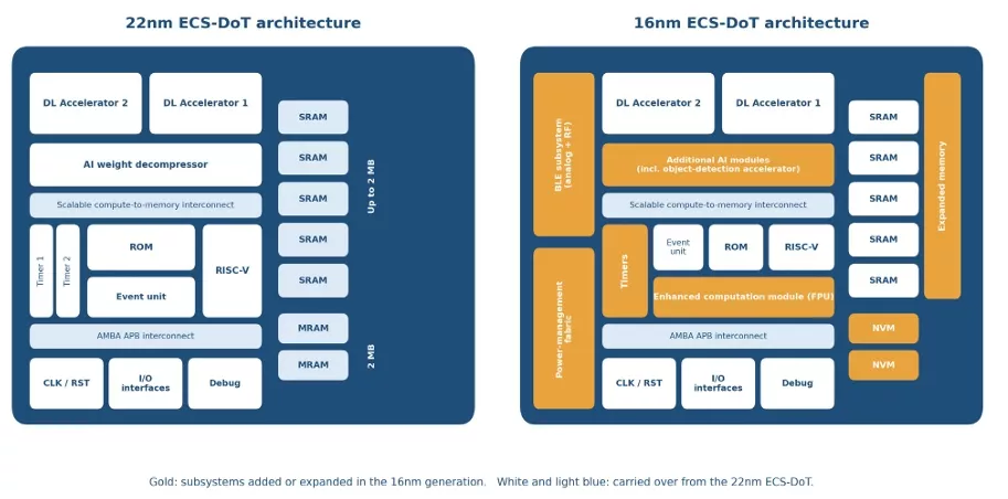
Figure 4: Block diagrams of the 22nm and 16nm ECS-DoT architectures. Subsystems added or expanded in the 16nm generation are shown in gold. Redrawn from the diagrams first published on 17 December 2025.
- Integrated Bluetooth Low Energy subsystem. The full BLE signal chain, including the analog front end, RF transceiver, phase-locked loops and on-chip matching networks, is built into the SoC. In many designs this removes the need for a separate wireless chip, cutting board area, bill-of-materials cost and design complexity for connected devices such as wearables, tags and industrial sensors.
- Expanded on-chip SRAM. A substantial increase in on-chip memory supports larger neural networks and higher-throughput vision and multi-sensor workloads, and reduces the off-chip memory accesses that dominate energy consumption in many edge AI systems.
- Adaptive fine-grained power-management fabric. EMASS’s most advanced power architecture to date, with fine-grained power gating across functional domains, dynamic clock gating and autonomous low-power states managed by internal controllers, giving microsecond-level sleep and wake behaviour for always-on monitoring in wearables, smart tags, industrial sensors and environmental monitoring. The design achieves this without dynamic voltage and frequency scaling, relying instead on architectural and circuit-level techniques.
- Dedicated AI acceleration module for object detection. A purpose-built engine for lightweight vision models such as YOLO-Nano class networks, MobileNet-SSD detection heads and FOMO-style detectors. It offloads detection from the main cores to raise throughput and cut inference latency in applications such as drones, smart cameras, safety systems and industrial inspection. The non-maximum suppression stage of this module is the subject of US Patent No. 12,651,452 B2, exclusively licensed to EMASS, as announced on 1 September 2026.
- Hardware floating-point unit. For the first time in the ECS-DoT family, the 16nm device includes an FPU supporting FP16 and FP32 operations. This speeds up digital signal processing and mixed-precision AI workloads and makes it simpler to port existing floating-point code and libraries to the platform.
Full software and workflow compatibility with the 22nm ECS-DoT is maintained across all of the above.
Next Steps: Bring-Up, Benchmarking and Characterisation
The engineering team will now take the samples through a structured program, the first stage of which is bring-up: powering the device, establishing communication with it and confirming that its core functions behave as designed. Once the chip is running, EMASS will move into benchmarking and characterisation across three areas:
- Functional behaviour and RF Characterisation. Functional testing of each on-chip subsystem, and characterisation of the integrated BLE radio, including transmit power, receive sensitivity and link performance, ahead of regulatory pre-compliance testing.
- Performance Benchmarking. Throughput and latency of the AI accelerators, the object-detection module and the FPU on standard edge AI models, and the behaviour of the expanded memory under larger networks.
- Power Measurement and Analysis. Measured active, idle and deep-sleep power, wake-up latency and energy per inference for representative vision, audio and sensor fusion workloads, compared against the 22nm device and against pre-silicon estimates.
When characterisation is complete, the Company will publish a summary of the measured power and performance of the 16nm ECS-DoT, based on silicon test data. The Company also intends, at that point, to make engineering samples and evaluation boards available to selected customers and partners.
Continuing to Smaller Nodes
Delivering an ultra-low-power edge AI SoC at 16nm FinFET demonstrates that EMASS can take the ECS-DoT architecture to an advanced node; the characterisation program will now quantify what the move delivers in power and performance. EMASS has now taken two designs through TSMC, at 22nm and 16nm, and has established the design, verification and physical design capability, including the recently established engineering centre in Cairo, to keep doing so. The Company continues to evaluate smaller process nodes for future generations of ECS-DoT, and intends to remain at the front of the category in bringing always on intelligence onto more advanced silicon.
Director of Nanoveu and Founder of EMASS, Dr Mohamed Sabry, said: “There is a particular moment in every chip program when the first parts come back from the fab and you can hold what was, until then, a set of files. We have reached that moment with the 16nm ECS-DoT. It carries everything we set out to build: the radio, the memory, the power fabric, the detection engine and the FPU, on one die at 16nm. Now the real work of measuring it starts, and we will report what the silicon tells us.”
Nanoveu will provide further updates as the 16nm ECS-DoT progresses through bring-up, benchmarking and characterisation.
About Nanoveu Limited
Further details on the Company can be found at https://nanoveu.com/.
EMASS is a fabless semiconductor company specialising in ultra-low-power, AI-enabled system-on-chip (SoC) solutions for always-on sensing and intelligent processing at the edge. Its ECS-DoT architecture enables real-time AI inference at milliwatt level power, supporting next-generation applications across drones, wearables, hearables, smart devices, industrial IoT, robotics and autonomous systems.
Spinoff is a Singapore-based aerial robotics company that designs and builds proprietary drone platforms. Its two current platforms are ALICE, a tethered aerial system engineered for high-payload, extended-duration operations with resistance to GPS and radio-frequency jamming and spoofing, and METRON, a camera-based 3D measurement system delivering millimetre-level precision with AI-driven deviation detection. Both platforms have been validated in commercial deployments with Tier-1 Singaporean customers. Spinoff Robotics provides Drone and sensing capabilities complementing the Company’s ECS-DoT edge-AI silicon across defence, critical-infrastructure security and industrial inspection markets.
EyeFly3D™ is a comprehensive platform solution for delivering glasses-free 3D experiences across a range of devices and industries. At its core, EyeFly3D™ combines advanced screen technology, sophisticated software for content processing, and the potential for integration with ultra-low-power SoC hardware.
Nanoshield™ includes protective and functional coating technologies designed for use across a range of applications, including solar and other industrial surfaces.
Related Semiconductor IP
- Generative AI Edge Processor
- AXI NoC Non-Coherent Mesh
- CXS c/d/Lite Verification IP
- USB OTG 2.0 with xHCI Verification IP
- DDR5 RDIMM Verification IP
Related News
- Hailo Selects Avnet ASIC as Channel Partner for TSMC Silicon Production
- AMD Achieves First TSMC N2 Product Silicon Milestone
- 2025 TSMC OIP Ecosystem Forum Highlights Aion Silicon’s Leadership in Advanced SoC Design
- Silicon Creations Announces 1000th Production FinFET Tapeout at TSMC and Immediate Availability of Full IP Library on TSMC N2 Technology
Latest News
- Agnisys and Axiomise Collaborate to Accelerate NoC Design and Formal Sign-off
- TSMC Reports Third Quarter EPS of NT$29.43
- ChipAgents Collaborates With NVIDIA to Launch Build-A-Chip-Bench for Autonomous Chip Design and Implementation
- Quintauris and Microchip Technology join forces to grow RISC-V® adoption
- BrainChip Launches Sequora: Edge AI That Doesn’t Just Recognize — It Understands and Responds