Overview
The Video Frame Buffer IP core buffers video data in external memory to be displayed on output devices such as computer monitors, projectors, etc. The Video Frame Buffer IP core supports image sizes up to 4Kx4K with YCbCr 4:2:2, 4:4:4 and RGB video formats. It supports dynamic parameter updating via a parameter bus which can be configured to operate on a different clock from the core. Simple frame rate conversion is employed to support different input and output frame rates.
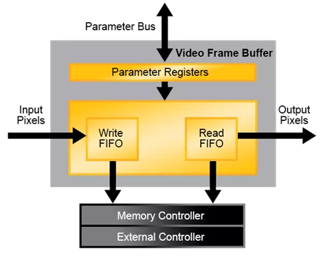
The Video Frame Buffer IP core receives input video data, stores it in the external memory and outputs it based on the timing controlled by the dout_enable signal. The core stores data into memory in a different width format as required by the application. It also provides synchronization of data across different clock domains as well as different format domains.
The core provides a simple parameter bus for dynamic frame size updating. It also implements a flexible memory interface that can be connected to Lattice memory controller IP cores.
The core also supports interlaced video stream by combining two fields into one frame outside.
The core supports continuous data streams from/to external interfaces in different clock domains using asynchronous Write and Read FIFOs. Input pixels are packed and stored into the asynchronous double clock Write FIFO first. Then pixels are sent to an external memory controller to be written to the memory. After an entire video frame has been stored in the external memory, frame reading starts. The pixels read from external memory are stored in the asynchronous Read FIFO and transferred to output interface clock domain. After unpacking, pixels are output from the Video Frame Buffer IP core.
In the video frame buffer, several clock sources are involved. The memory interface operates on a separate memory clock. When frame rate conversion is enabled, there are two clocks in the video data path: input pixel sample clock and output pixel sample clock. When frame rate conversion is disabled, the video data path oper-ates at input pixel sample clock rate. When dynamic parameter updating is enabled, the parameter bus can be configured to run on a separate clock. By default, the parameter bus runs on the input pixel sample clock.
Learn more about Video Processing IP core
Extending Lattice's post-quantum cryptography leadership from silicon to a complete platform security stack, Lattice Sentry now delivers CNSA 2.0-aligned, NIST-compliant protection across AI data centers, and critical infrastructure, giving system designers a validated, production-ready path to quantum-resistant security.
Combining Arm® AGI CPU server platforms with Lattice FPGAs and AMI firmware creates a solution that provides advanced security, manageability, connectivity, and flexibility for next-generation AI data center infrastructure.
Lattice Prompt pairs with AI agentic tools developers already use, combining them with Lattice design tools, knowledge base, and documentation to turn natural language inputs into validated responses, dramatically accelerating FPGA development while optimizing design performance and capability.
First announced on May 4, 2026, the acquisition creates the industry's most complete secure management and control platform.
The acquisition brings together Lattice’s industry-leading low power FPGAs with AMI’s industry‑leading platform firmware and infrastructure manageability solutions for cloud and AI to create a complete portfolio of secure management and control solutions.
The collaboration demonstrates a real-time AI sensor fusion architecture that integrates TI mmWave radar and camera sensors using NVIDIA Holoscan Sensor Bridge running on Lattice’s low power FPGA. The FPGA acts as a companion chip delivering synchronized sensor data directly into GPU-accessible memory to enable low-latency and robust perception for robotics and industrial edge AI applications.