Universal Chiplet Interconnect Express (UCIe™) PHY and Controller
High-bandwidth, low-power and low-latency standardized die-to-die interconnect
Overview
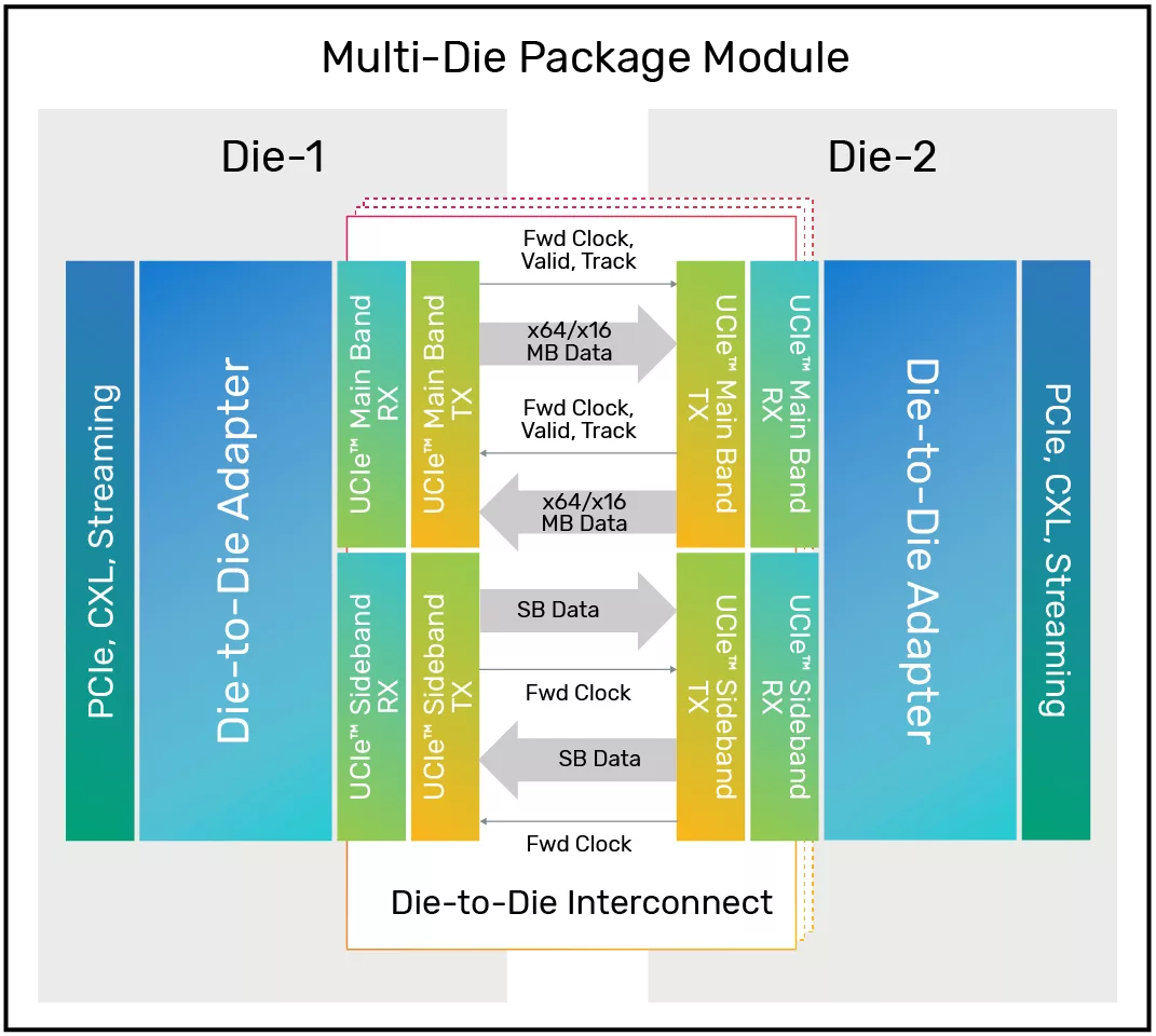
The Cadence UCIe™ PHY is a high-bandwidth, low-power and low-latency die-to-die solution that enables multi-die system in package integration for high performance compute, AI/ML, 5G, automotive and networking applications. The UCIe™ physical layer includes the link initialization, training, power management states, lane mapping, lane reversal, and scrambling. The UCIe™ controller includes the die-to-die adapter layer and the protocol layer. The adapter layer ensures reliable transfer through link state management and parameter negotiation of the protocol and flit formats. The UCIe™ architecture supports multiple standard protocols such as PCIe, CXL and streaming raw mode.
Key features
PHY
- Supports up to 32Gbps per pin including 4/8/12/16/24Gbps
- Forwarded clock, track, and valid pins
- Sideband messaging for link training and parameter exchange
- KGD (Known Good Die) testing capability
- Redundant lane repair (advanced)
- Width degradation (standard)
- Lane reversal
- Supports advanced and standard package designs with up to 25mm channel reach
- Silicon measured low raw BER as low as 1E-27 compared to spec of 1E-15
- Simplified clock management with integrated PLL
- Hardware-bringup with no firmware required
Controller
- Lowest latency controller for data intensive die-to-die applications
- Supports single and multiple PHY modules
- CXS, CHI C2C, AXI, PCIe, CXL, and streaming protocols
- CRC and retry mechanism
- Sideband messaging for link training, parameter exchange, and vendor defined messages
- Link State Management
- Parameter Negotiation
Block Diagram
Benefits
- Package Flexibility: Supports standard package (2D) and advanced package (2.5D)
- Power Efficiency: Advanced architecture meets ultra-low power requirements
- Low Latency: For data-intensive applications
- High Performance Reliability: Efficient design for maximum die-to-die throughput and link data integrity
- Multi-protocol Solution: Supports CXS, CHI C2C, AXI, PCIe, CXL, and streaming protocols
- Interoperability: KGD and robust test methods ensure seamless link reliability
Specifications
Identity
Files
Note: some files may require an NDA depending on provider policy.
Provider
Learn more about UCIe IP core
The Next-Generation UCIe IP Subsystem for Advanced Package Designs
Cadence Silicon Success of UCIe IP on Samsung Foundry’s 5nm Automotive Process
Advancing Die-to-Die Connectivity: The Next-Generation UCIe IP Subsystem
Cadence Sets the Gold Standard for UCIe Connectivity at Chiplet Summit '24
UCIe Interoperability Between Intel and Cadence
Frequently asked questions about UCIe IP cores
What is Universal Chiplet Interconnect Express (UCIe™) PHY and Controller?
Universal Chiplet Interconnect Express (UCIe™) PHY and Controller is a UCIe IP core from Cadence Design Systems, Inc. listed on Semi IP Hub.
How should engineers evaluate this UCIe?
Engineers should review the overview, key features, supported foundries and nodes, maturity, deliverables, and provider information before shortlisting this UCIe IP.
Can this semiconductor IP be compared with similar products?
Yes. Buyers can compare this product with similar semiconductor IP cores or IP families based on category, provider, process options, and structured technical specifications.