Overview
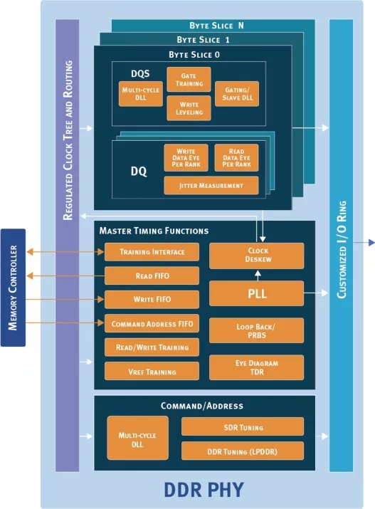
The TCI DDR PHY is a high-performance, scalable system using a radically new architecture that continuously and automatically adjusts each pin individually, correcting skew within byte lanes. This state-of-the-art tuning acts independently on each pin, data phase and chip select value. Read gate and data eye timing are also continuously adjusted. Automatic training is included for multi-cycle write leveling and read gate timing, read/write data eye timing, and PHY Vref and DRAM Vref settings. Remarkable physical flexibility allows the PHY to adapt to each customer’s die floorplan and package constraints, yet is delivered and verified as a single unit for easy timing closure with no assembly required. The PHY is DFI 5.1 compliant, and when combined with an appropriate DDR memory controller, a complete and fully-automatic DDR system is realized.
Learn more about DDR IP core
Students and researchers now have easy access to quality IP and MPW services through Muse
True Circuits, Inc. (TCI), a leading provider of analog and mixed-signal intellectual property (IP) and developer of computer aided design (CAD) software announced today its intention to donate the JSPICE Design Environment (JDE) to form the foundation of a modern AMS development environment that unifies design generation, simulation, measurement, characterization, data analysis, and AI-assisted engineering into a single extensible environment.
The Ultra+ PLL is designed as an ultra-low jitter, extremely wide range clock multiplier with precise fractional frequency control and optional spread spectrum capability, giving chip designers the ultimate in performance, features and ease of use.
At the 62nd Design Automation Conference (DAC), True Circuits will introduce an improved, state-of-the-art digital LC PLL that includes an innovative digital control algorithm that cuts the lock time by as much as 70% over previous versions, while directly controlling the loop bandwidth accurately (by 0.1% of Fref or better) and consistently across PVT variations through continuous background loop-gain calibration.
TCI will introduce its powerful JSPICE™ Design Environment (JDE™) which has been used by True Circuits over the last 26 years to create complex analog and digital IP and will now be available to the public through a membership program.
At the 60th Design Automation Conference (DAC), TCI will introduce its powerful JSPICE™ simulation and design environment which has been used by True Circuits over the last 25 years to create complex analog and digital IP and will now be available to the public initially through a beta test.