Vendor: Arasan Chip Systems Inc. Category: SD / eMMC Controller

SD 4.1 Hardware Validation Platform

The rapid proliferation of high-performance mobile and handheld devices has resulted in increasing requirements for non-volatile …

Overview

The rapid proliferation of high-performance mobile and handheld devices has resulted in increasing requirements for non-volatile memory. Memory interfaces with larger capacities and faster access times are needed.

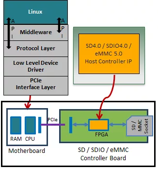
The SD memory card interface dominates the mobile storage markets such as tablets, smartphones, video camcorders, and many other portable or stationary consumer electronics. Designed to be cost-effective and Linux based, this SD 4.1 hardware validation platform (HVP) consists of Arasan’s SD4.0 IP mapped into FPGA’s, offering full speed physical connectivity to a complementary SoC host or memory card device. Owing to its active participation in the SDA standards body, and being the first to market SD controller IP, Arasan’s SD controller IP implementation is considered a reference implementation in the industry.

An equally important part of the SD 4.1 HVP is the software stack, which abstracts all the low-level software drivers and hardware to a loadable shared object with easy to use API’s. Hence, an applications software, validation or systems engineer does not need to delve into the protocol and signaling details and considers the Arasan platform as a programmable complementary device. The SD 4.1 HVP can be used by system developers, system integrators, software developers and system quality analysts to debug as well as validate their products during the product life-cycle.

Key features

Compliance

  • Supports SD host controller standard spec v 3.0/4.0
  • Supports SD Physical Spec v 3.0/4.0 & UHS-II addendum
  • Supports SDIO Card Spec v 3.0/4.0
  • Supports Embedded SD Physical Spec v 2.1

SDIO/SD/SDHC/SDXC/UHS-I/UHS-II/eSD Device Validation
  • Sub-LVDS differential signaling compliant with UHS-II specification
  • Supports serial transmission in Full-duplex mode from 390 to 780 Mbps each lane, and Half-duplex mode up to 1.5 Gbps
  • Using 8b/10b encoding for data transmission
  • Low frequency differential RCLK at 1/15th or 1/30th of data rate
  • Multiple power saving modes: Dormant, Line Standby
  • Drives RCLK (52Mhz) for SD Device to generate its clock
  • Supports Data Retries, Boot Code Loading, Bus Master with Scatter Gather DMA
  • CRC16 integrity check for Data and Command
  • Card detection (Insertion / Removal)
  • Host clock rate variable between 0 and 208 MHz
  • Supports SD 1/4-bit and SDIO 1/4-bit modes
  • Direct and extended read/write (IO52, IO53) transactions

Block Diagram

What’s Included?

  • SD/SDIO/eMMC Validation Platform including:
  • SD 4.0/SDIO 4.0/eMMC 5.0 Controller IP implemented in FPGA
  • SD Software Stack
  • Linux Installer Package with Documentation
  • Documentation


Specifications

Identity

Part Number
SD 4.1 Hardware Validation Platform
Vendor
Arasan Chip Systems Inc.
Type
Silicon IP

Files

Note: some files may require an NDA depending on provider policy.

Provider

Learn more about SD / eMMC Controller IP core

UFS Goes Mainstream

UniversalFlash Storage (UFS) was created for mobile applications and computer systems requiring high performance and low power consumption. These systems typically use embedded Flash based on the JEDEC standard eMMC. UFS was defined by JEDEC as the evolutionary replacement for eMMC offering significantly higher memory bandwidth. The standard builds on existing standards such as the SCSI command set, the MIPI Alliance M-PHY and UniPro as well as eMMC form factors to simplify adoption and development.

Universal Flash Storage: Mobilize Your Data

Universal Flash Storage (UFS) was created for mobile applications and computer systems requiring high performance and low power consumption. These systems typically use embedded Flash based on the JEDEC standard eMMC. UFS was defined by JEDEC as the evolutionary replacement for eMMC offering significantly higher memory bandwidth. The standard builds on existing standards such as the SCSI command set, the MIPI Alliance M-PHY and UniProSM as well as eMMC form factors to simplify adoption and development.

Types of Storages for Computing System-On-Chips

We are living in an age where we generate the same amount of data each year that has been generated since antiquity. Ever wondered how and where these peta /exa/zetta bytes of data are stored?

Virtual Prototyping Platform with Flash Memory

In this paper we will see how the flash memories developed using Carbon Model Studio helps to bring up an ARM® Cortex A7 flash memory sub-system with primary and secondary boot codes. Flash memories system demonstrated here can be used for early boot code and driver development for any CPU based SoC.

Frequently asked questions about SD / eMMC Controller IP cores

What is SD 4.1 Hardware Validation Platform?

SD 4.1 Hardware Validation Platform is a SD / eMMC Controller IP core from Arasan Chip Systems Inc. listed on Semi IP Hub.

How should engineers evaluate this SD / eMMC Controller?

Engineers should review the overview, key features, supported foundries and nodes, maturity, deliverables, and provider information before shortlisting this SD / eMMC Controller IP.

Can this semiconductor IP be compared with similar products?

Yes. Buyers can compare this product with similar semiconductor IP cores or IP families based on category, provider, process options, and structured technical specifications.

×
Semiconductor IP