QDR2 Memory Model
QDR2 Memory Model provides an smart way to verify the QDR2 component of a SOC or a ASIC.
Overview
QDR2 Memory Model provides an smart way to verify the QDR2 component of a SOC or a ASIC. The SmartDV's QDR2 memory model is fully compliant with standard QDR2 Specification and provides the following features. Better than Denali Memory Models.
QDR2 Memory Model is supported natively in SystemVerilog, VMM, RVM, AVM, OVM, UVM, Verilog, SystemC, VERA, Specman E and non-standard verification env
QDR2 Memory Model comes with optional Smart Visual Protocol Debugger (Smart ViPDebug), which is GUI based debugger to speed up debugging.
Key features
- Supports QDR2 memory devices from all leading vendors.
- Supports 100% of QDR2 protocol standard CY7C1314CV18.
- Supports for Separate independent read and write data ports with concurrent read and write operation
- Supports for Full data coherency, providing most current data.
- Supports for Synchronous pipeline read with self-timed late write.
- Supports for Registered address, control and data input/output.
- Supports for QDR (Double Data Rate) Interface on read and write ports.
- Supports for Fixed 4-bit burst for both read and write operation.
- Clock-stop supports to reduce current.
- Supports for Two input clocks (K and K) for accurate QDR timing at clock rising edges only.
- Supports for Two input clocks for output data (C and C) to minimize clock-skew and flight-time mismatches.
- Supports for Two echo clocks (CQ and CQ) to enhance output data traceability.
- Supports for Single address bus.
- Supports for Byte write function.
- Supports for Simple depth expansion with no data contention.
- Supports for Programmable output impedance.
- Supports for Single Multiplexed Address Input Bus latches Address Inputs for both Read and Write Ports
- Supports for Separate Port Selects for Depth Expansion
- Supports for Synchronous internally Self-timed Writes
- QDR II operates with 1.5 Cycle Read Latency when Delay Lock Loop (DLL) is enabled
- Operates similar to a QDR I Device with one Cycle Read Latency in DLL Off Mode
- Supports for Available in x18, and x36 Configurations
- Supports for Variable Drive HSTL Output Buffers
- Supports all the QDR2 commands as per the specs.
- Supports for Delay Lock Loop (DLL) for accurate Data Placement
- Supports for full-timing as well as behavioral versions in one model.
- Supports for all timing delay ranges in one model: min, typical and max.
- Protocol checker fully compliant with QDR2 Specification CY7C1314CV18.
- Models, detects and notifies the test bench of significant events such as transactions, warnings, and timing protocol violations.
- Notifies the test bench of significant events such as transactions, warnings, timing and protocol violations.
- Constantly monitors QDR2 behavior during simulation.
- Built in functional coverage analysis.
- Supports Callbacks, so that user can access the data observed by monitor.
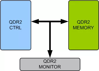
Block Diagram
Benefits
- Faster testbench development and more complete verification of QDR2 designs.
- Easy to use command interface simplifies monitor control and configuration.
- Simplifies results analysis.
- Runs in every major simulation environment.
What’s Included?
- Complete regression suite containing all the QDR2 testcases.
- Examples showing how to connect and usage of Model.
- Detailed documentation of all class, task and function's used in verification env.
- Documentation also contains User's Guide and Release notes.
Specifications
Identity
Files
Note: some files may require an NDA depending on provider policy.
Provider
Learn more about SRAM IP core
Novel Trade-offs in 5 nm FinFET SRAM Arrays at Extremely Low Temperatures
Why SRAM PUF Technology Is the Bedrock of Dependable Security in Any Chip
AI-driven SRAM demand needs integrated repair and security
A comparison of SRAM vs quantum-derived semiconductor PUFs
Basics of SRAM PUF and how to deploy it for IoT security
Frequently asked questions about SRAM IP cores
What is QDR2 Memory Model?
QDR2 Memory Model is a SRAM IP core from SmartDV Technologies listed on Semi IP Hub.
How should engineers evaluate this SRAM?
Engineers should review the overview, key features, supported foundries and nodes, maturity, deliverables, and provider information before shortlisting this SRAM IP.
Can this semiconductor IP be compared with similar products?
Yes. Buyers can compare this product with similar semiconductor IP cores or IP families based on category, provider, process options, and structured technical specifications.