PCIe 3.1 Controller
The PCIe 3.1 Controller (formerly XpressRICH) is designed to achieve maximum PCI Express (PCIe) 3.1 performance with great design…
Overview
The PCIe 3.1 Controller (formerly XpressRICH) is designed to achieve maximum PCI Express (PCIe) 3.1 performance with great design flexibility and ease of integration. It is fully compatible with the PCIe 3.1/3.0 specification. A PCIe 3.1 Controller with AXI (formerly XpressRICH-AXI) is also available. The controller delivers high-bandwidth and low-latency connectivity for demanding applications in data center, edge and graphics.
How the PCIe 3.1 Controller Works
The PCIe 3.1 Controller is configurable and scalable IP designed for ASIC and FPGA implementation. It supports the PCIe 3.1/3.0 specifications, as well as the PHY Interface for PCI Express (PIPE) specification. The IP can be configured to support endpoint, root port, switch port, and dual-mode topologies, allowing for a variety of use models.
The provided Graphical User Interface (GUI) Wizard allows designers to tailor the IP to their exact requirements, by enabling, disabling, and adjusting a vast array of parameters, including data path size, PIPE interface width, low power support, SR-IOV, ECC, AER, etc. for optimal throughput, latency, size and power.
The PCIe 3.1 Controller is verified using multiple PCIe VIPs and test suites, and is silicon proven in hundreds of designs in production. Rambus integrates and validates the PCIe 3.1 Controller with the customer’s choice of 3rd-party PCIe 3.1 PHY.
Key features
- PCI Express layer
- Compliant with the PCI Express 3.1/3.0, and PIPE (16- and 32-bit) specifications
- Compliant with PCI-SIG Single-Root I/O Virtualization (SR-IOV) Specification
- Supports Endpoint, Root-Port, Dual-mode, Switch port configurations
- Supports x16, x8, x4, x2, x1 at 8 GT/s, 5 GT/s, 2.5 GT/s speeds
- Supports AER, ECRC, ECC, MSI, MSI-X, Multi-function, crosslink, and other optional features
- Additional optional features include OBFF, TPH, ARI, LTR, IDO, L1 PM substates, etc.
- User Interface layer
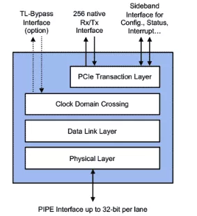
- 256-bit transmit/receive low-latency user interface
- User-selectable Transaction/Application Layer clock frequency
- Sideband signaling for PCIe configuration access, internal status monitoring, debug, and more
- Optional Transaction Layer bypass
Block Diagram
What’s Included?
- IP files
- Verilog RTL source code
- Libraries for functional simulation
- Configuration assistant GUI
- Documentation
- PCI Express Bus Functional Model
- Encrypted Simulation libraries
- Software
- PCI Express Windows x64 and Linux x64 device drivers
- PCIe C API
- Reference Designs
- Synthesizable Verilog RTL source code
- Simulation environment and test scripts
- Synthesis project & DC constraint files (ASIC)
- Synthesis project & constraint files for supported FPGA hardware platforms (FPGA)
Specifications
Identity
Standards & Interfaces
Files
Note: some files may require an NDA depending on provider policy.
Provider
Learn more about PCI Express IP core
PCI Express 5 vs. 4: What's New? [Everything You Need to Know]
Complete Interface Solution for PCI Express 5.0 Launched
Challenges in PCI Express IP Implementation
Bulletproofing PCIe-based SoCs with Advanced Reliability, Availability, Serviceability (RAS) Mechanisms
PCIe 5.0 Controller IP on FPGAs: Current and Future Use Cases
Frequently asked questions about PCIe IP cores
What is PCIe 3.1 Controller?
PCIe 3.1 Controller is a PCI Express IP core from Rambus, Inc. listed on Semi IP Hub.
How should engineers evaluate this PCI Express?
Engineers should review the overview, key features, supported foundries and nodes, maturity, deliverables, and provider information before shortlisting this PCI Express IP.
Can this semiconductor IP be compared with similar products?
Yes. Buyers can compare this product with similar semiconductor IP cores or IP families based on category, provider, process options, and structured technical specifications.