Vendor: Innosilicon Technology Ltd Category: DDR

ONFI PHY & Controller

The ONFI IP provides Turnkey solutions for IC requiring access to ONFI-compatible NAND Flash devices.

Controller + PHY View all specifications

Overview

The ONFI IP provides Turnkey solutions for IC requiring access to ONFI-compatible NAND Flash devices. Optimized for low power and high-speed applications, it features robust timing and a compact silicon area. It supports all ONFI NAND Flash components available on the market. The PHY includes critical timing synchronization modules (TSM) specialized for utility and functionality and low power/jitter DLLs with programmable fine-grain control for any NAND Flash interface.

The AXI interface ONFI provides four AXI channels to connect to the ONFI PHY, ensuring compliance with the DFI digital interface specifications. It employs a two-layer architecture, making the interface flexible and easily adaptable to various multi-port bus formats and timing sequences. One layer consists of the CPU bus core, which supports single or a multi-port CPU buses, while the other layer is the controller core responsible for communication with the DFI PHY. Between these layers, the TX/RX data FIFOs and a generic command FIFO are utilized to isolate the internal controller from changes of the CPU bus core.

The overall design of the IP solution is versatile, lightweight, and easily adjustable to different CPU bus ports. It achieves high efficiency within a compact design. All interface timings on DFI and controller are in 1x SDR clock domain which can run at half the speed of the PHY core. The interface is highly generic and supports high-performance input and output data flow, reaching up to 4800Mbps ONFI speeds in a wide range.

Key features

  • ONFI5.1 modes & signaling, rates up to 4800Mbps
  • x8/x16 data path interface extendable
  • Supports 1.2 V/1.8V I/Os
  • Multiple drive strengths adjustable
  • Independent DCC training, Vref training for NV-DDR3/NV-LPDDR4
  • Independent read and write timing adjustments with auto calibration for NV-DDR3/NV-LPDDR4
  • Low latency with programmable timings for secure data handling
  • Per-bit deskew support
  • Supports point to point memory subsystems, multi-host, and multi-channel
  • PVT compensation and timing calibration for all corner reliability
  • At speed BIST, scan insertion
  • Various power-down modes for low power
  • Low jitter with superior noise rejection
  • APB Port register access interface
  • Supports both wire-bond and flip- chip packaging
  • Wire-bond speed is package limited
  • Supports different signal mappings for feasible PCB layout

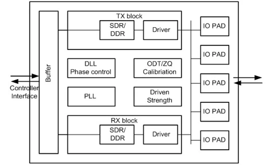
Block Diagram

Benefits

  • Fully pre-assembled design, Drop-in hard macro to ease integration and speed time to market
  • Zero risk with robust ESD architecture
  • Extensive EDA tool support for various design and automation flow
  • Optional CKE retention mode permits VDD and all non-essential I/Os to be powered down while retaining the external SDRAMs in self-refresh mode
  • Flexible pad ring configuration to adapt for various design and chip scenarios
  • Takes full advantage of process savings and speed capability
  • Comprehensive observation registers DFX and methods are available to facilitate customers in identifying issues during testing

What’s Included?

  • Extensive documentation
  • Models
  • LIB
  • LEF
  • Place-and-route abstracts
  • LVS netlist
  • GDSII files

Specifications

Identity

Part Number
ONFI
Vendor
Innosilicon Technology Ltd
Type
Silicon IP
Controller / PHY
Controller + PHY

Files

Note: some files may require an NDA depending on provider policy.

Provider

Learn more about DDR IP core

PCIe 5.0: The universal high-speed interconnect for High Bandwidth and Low Latency Applications Design Challenges & Solutions

Innosilicon, a leading IP provider, offers a complete PCIe 5.0 solution stack that includes both PHY and controller IPs. Although both layers are crucial to achieving a fully compliant and high-performance PCIe interface, this paper deep dives into the technical challenges of PHY design, highlighting insights drawn from real-world design margins, receiver robustness, and advanced jitter analysis in the context of Gen5 systems.

Frequently asked questions about DDR Interface IP

What is ONFI PHY & Controller?

ONFI PHY & Controller is a DDR IP core from Innosilicon Technology Ltd listed on Semi IP Hub.

How should engineers evaluate this DDR?

Engineers should review the overview, key features, supported foundries and nodes, maturity, deliverables, and provider information before shortlisting this DDR IP.

Can this semiconductor IP be compared with similar products?

Yes. Buyers can compare this product with similar semiconductor IP cores or IP families based on category, provider, process options, and structured technical specifications.

×
Semiconductor IP