Overview
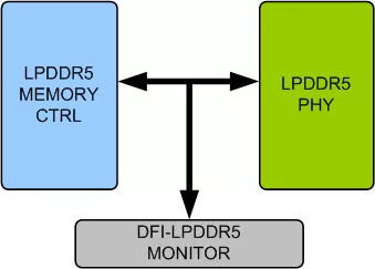
LPDDR5 DFI Verification IP provides an smart way to verify the LPDDR5 DFI component of a SOC or a ASIC. The SmartDV's LPDDR5 DFI Verification IP is fully compliant with standard DFI Specification and provides the following features.
LPDDR5 DFI Verification IP is supported natively in SystemVerilog, VMM, RVM, AVM, OVM, UVM, Verilog, SystemC, VERA, Specman E and non-standard verification env
LPDDR5 DFI Verification IP comes with optional Smart Visual Protocol Debugger (Smart ViPDebug), which is GUI based debugger to speed up debugging.
Learn more about Protocol Bridge IP core
This collaboration combines SmartDV’s production-proven IP with Mirabilis Design’s VisualSim® system-level modeling platform to provide customers with fully validated architectural models that reflect real implementation behavior.
Comprehensive support for both MIPI SoundWire I3S 1.0 and draft 1.1 specifications delivers flexible, standards-aligned integration for advanced audio, voice, and control subsystems
As the Compute Express Link® (CXL®) specification rapidly evolves, so too must the tools and infrastructure used to verify designs built around it. Maintaining verification IP (VIP) that keeps pace with new specification revisions is no small task, particularly when dealing with major version shifts like the transition from CXL 2.0 to 3.0.
SmartDV supports all three profiles of each technology: Baseline, Main, and High for H.264, and Main, Main 10, and Main Still Picture for H.265, enabling seamless integration and unparalleled flexibility for developers across diverse applications.
To meet RANiX’s unique design goals, SmartDV will customize the IP to go beyond the standard SDIO functionality—thereby empowering RANiX to differentiate from their competitors. SmartDV will also provide RANiX with the requisite support and documentation to achieve ASIL certification for ISO 26262.
SmartDV™ Technologies, provider of flexible, customizable semiconductor design IP (intellectual property) and verification solutions, has expanded engineering operations beyond its headquarters in Bengaluru with the opening of a new office space in Coimbatore, Tamil Nadu, India.