Overview
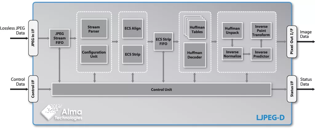
The LJPEG-D core is a matching decoder for the LJPEG-E Lossless JPEG encoder from Alma Technologies and supports up to 16-bit per component Numerically Lossless decoding. Coupled with the LJPEG-E, the decoder is ideal for image and video compression applications where bit-by-bit accurate reproduction of an image is essential, while the amount of compression needed is very low.
The LJPEG-D is based on the spatial (sequential) lossless compression mode (SOF3) of the ISO/IEC 10918-1 JPEG standard. Rather than the Discrete Cosine Transform (DCT) functions used for lossy JPEG compression - which introduce round-off errors - Lossless JPEG employs a predictor function and compresses images by encoding the prediction error with no information loss.
The core is designed with simple, fully flow-controllable and FIFO-like, streaming input and output interfaces. Being carefully designed, rigorously verified and silicon-proven, the LJPEG-D is a compact, reliable and easy-to-use and integrate IP.
Learn more about Image Conversion IP core
Alma Technologies S.A. today announced its new UHT-SCALER IP core, a standalone and high-performance image scaler, designed for enabling ultra-high frame rate SD, HD or Ultra HD (4K/8K and beyond) image resizing, even in low-end ASIC or FPGA silicon.
Alma Technologies S.A. today announced its new UHT-JPEGLS-E scalable encoder IP core that enables numerically lossless encoding of ultra-high frame rate SD/HD, and Ultra HD video (4K/8K and beyond), even in highly cost-effective FPGA and ASIC technologies.
Alma Technologies S.A. today announced its new UHT-DSC-E and UHT-DSC-D DSC 1.2b encoder and decoder IP cores that enable the transport of high-definition content with up to 10K resolution, 120Hz refresh rate, high dynamic range and high color depth through existing interfaces, such as VESA DisplayPort, MIPI DSI and HDMI 2.1.
This new scalable UHT JPEG 2000 encoder IP core provides the extreme performance needed by modern video compression applications that have to cope with massive pixel rates and resolutions.
An online tool for back-to-back comparison of the image compression standards implemented by our IP cores is now available on our website. The Bit Accurate Models of the respective image compression cores are used to encode / decode a user supplied test image, in order to evaluate and compare their actual performance.
Alma Technologies S.A., a company that designs, markets, sells and supports innovative semiconductor IP since 2001, today introduced at the Toulouse Space Show 2016 a new encoder IP core which implements the CCSDS 122.0-B-1 lossless and lossy image data compression standard.