CDM Dependence on Device Capacitance
This blog will focus on what happens during the CDM pulse itself, and will show how the pulse properties change as a function of DUT to Field Plate capacitance.
A TSMC 130nm Wirebond/Flipchip compatible I/O Library with 5V GPIO, 5V ODIO, 5V Analog I/O and 5V Power Supply I/O.
A TSMC 130nm Wirebond/Flipchip compatible I/O Library with 5V GPIO, 5V ODIO, 5V Analog I/O and 5V Power Supply I/O.
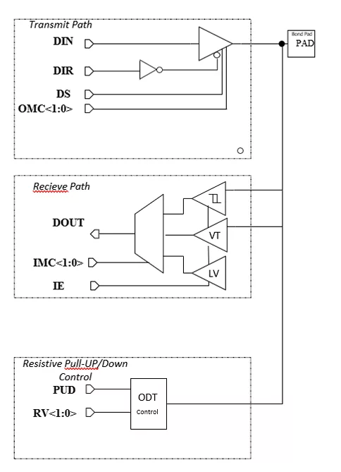
This silicon-proven, I/O Library features a 5V General Purpose I/O, 5V Open-Drain I/O, 5V Analog I/O, 5V Power Supply and an area efficient 5V ESD protection scheme. The functional cells in the library (GPIO & ODIO) feature an Output Enable pin which, when de-asserted, place the I/O in a HiZ state, and can control multiple modes of output operation with the Output Mode Control pins. The input RX path for this library all have selectable operations between a Schmitt trigger input with hysteresis, a standard buffer with no hysteresis, and a low input voltage mode that can receive a voltage level much lower than the I/O supply without causing metastability or large leakage current. The library has no poly orientation limitations and can be used in any orientation. The library cells are only built up to metal three, but include an metal 4 pad anchor that can be overlaid with either a wirebond or connected to a BUMP. ESD design level are 2kV HBM, 500V CDM and +/-125mA Latch-up.
Operating Conditions
| Parameter | Value |
| VDDIO | 1.1V to 5.5V |
| Core VDD | 1.71V to 5.5V |
| BEOL | 1P4M |
| Temperature | –40C to 125C |
| ESD | 2kV HBM & 500V CDM |
Cell Summary
| Cell Type | Cell Size |
| GPIO | 120um x 75um |
| ODIO | 98um x 55um |
| GPI | 118um x 55um |
| ESD IO | 35um x 55um |
| ESD VCC | 35um x 55um |
| ESDRC IO | 50um x 55um |
| ESDRC VCC | 50um x 55um |
| ESDRC IO2 | 171.32um x 55um |
| ESDRC VCC2 | 171.32um x 55um |
| Foundry | Node | Process | Maturity |
|---|---|---|---|
| TSMC | 130nm | BCD/BCD+ | — |
Note: some files may require an NDA depending on provider policy.

I/O Library in TSMC 130nm 5V Gen3 BCD is a GPIO IP core from Certus Semiconductor listed on Semi IP Hub. It is listed with support for tsmc.
Engineers should review the overview, key features, supported foundries and nodes, maturity, deliverables, and provider information before shortlisting this GPIO IP.
Yes. Buyers can compare this product with similar semiconductor IP cores or IP families based on category, provider, process options, and structured technical specifications.