Simplifying Multi-Domain Voltage-Control Verification with Synopsys AVSBus 2.0 VIP
Learn how AVSBus 2.0 VIP validates power delivery in AI and data center SoCs.
The HBM3 PHY is a physical layer IP interface (PHY) solution for high-performance computing (HPC), AI, graphics, and networking A…
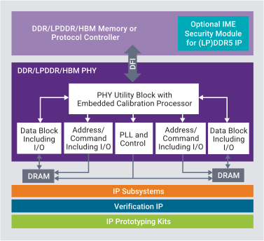
The HBM3 PHY is a complete physical layer IP interface (PHY) solution for high-performance computing (HPC), AI, graphics, and networking ASIC, ASSP, and system-on-chip (SoC) applications requiring high-bandwidth HBM3 DRAM interfaces operating at up to 9600 Mbps. The HBM3 PHY offers superior power efficiency compared to any other off-chip memory interface and supports up to 4 active operating states enabling dynamic frequency scaling. To minimize area, the PHY utilizes an optimized micro bump array. Support for longer channel lengths allows more flexibility in the PHY placement on the SoC without impacting performance. The PHY provides a complete HBM3 interface solution when combined with HBM3 Controller IP and HBM3 memory model VIP.
The configurable HBM3 PHY is provided as a set of hard macrocells delivered as GDSII. These hard macrocells include integrated application-specific HBM3 I/Os required for HBM3 signaling. The design is optimized for high performance, low latency, low area, low power, and ease of integration. The hard macrocells are easily assembled into a complete 1024-bit HBM3 PHY. The RTL-based PHY Utility Block (PUB) supports the GDSII-based PHY components and includes the PHY training circuitry, configuration registers, and BIST control. The HBM3 PHY includes a DFI 5.0-compatible interface to the memory controller, supporting DFI DFI 1:1:2, DFI 1:2:4 and DFI 1:4:8 clock ratios. The design is compatible with both metal-insulator-metal (MIM) and non-MIM power decoupling strategies. The the vendor also offers a pre-hardened “drop-in” version of the HBM3 PHY for customers who do not have significant custom requirements. For customers that require a custom hard HBM3 PHY, the vendor also offers PHY hardening design services.
Note: some files may require an NDA depending on provider policy.

HBM3 PHY - TSMC N5 1.2V is a HBM IP core from Synopsys, Inc. listed on Semi IP Hub.
Engineers should review the overview, key features, supported foundries and nodes, maturity, deliverables, and provider information before shortlisting this HBM IP.
Yes. Buyers can compare this product with similar semiconductor IP cores or IP families based on category, provider, process options, and structured technical specifications.