HBM2E/HBM2 PHY
Highest performance IP for graphics, AI/ML
Overview
The Cadence High-Bandwidth Memory generation 2/2E PHY (HBM2E/2 PHY) is silicon-proven and is available in four process nodes: PHYs, achieving breakthrough performance, low energy per bit, and low area relative to the data bandwidth. It is engineered to quickly and easily integrate into SoCs and is verified as part of a complete memory subsystem solution. The HBM2E/2 PHY IP is an ideal solution for artificial intelligence (AI), high-performance computing (HPC), and image processing applications.
Key features
PHY
- Advanced clocking architecture minimizes clock jitter
- DFI PHY Independent Mode for initialization and training
- IEEE 1500 interface, Memory BIST feature, and loop-back function
- Designed for optimized interposer routing
- Pin programmable support for lane repair
Controller
- High-performance command queue placement and command execution selection
- Optimized throughput of unique pseudo-channel interleaving
- Lowest latency for data-intensive applications
- Low-power control and advanced low-power modes with power-down and self-refresh
- Memory controller interface is based on DFI 5.0
- DFI frequency ratio of 2:1
- Memory BIST feature
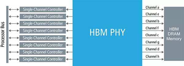
Block Diagram
Benefits
- Proven: Silicon characterization reports available
- Low Latency: For data-intensive applications
- High Performance: Highest performance HBM2E at 3.6Gbps. Interposer optimized for best signal integrity.
- Low Power and Area: Low power control: advanced low power modes
Applications
- Communications,
- Consumer Electronics,
- Data Processing,
- Industrial and Medical,
- Military/Civil Aerospace
What’s Included?
- GDS II macros with abstract in LEF
- Verilog post-layout netlist
- STA scripts for use at chip or standalone PHY levels
- Liberty Timing model
- SDF for back-annotated timing verification
Silicon Options
| Foundry | Node | Process | Maturity |
|---|---|---|---|
| Samsung | 10nm | LPP | Available on request |
Specifications
Identity
Files
Note: some files may require an NDA depending on provider policy.
Provider
Learn more about HBM IP core
The Memory Imperative for Next-Generation AI Accelerator SoCs
Heterogeneous Multicore using Cadence IP
Cadence Powers AI Infra Summit '25: Memory, Interconnect, and Interface Focus
Designing the AI Factories: Unlocking Innovation with Intelligent IP
HBM4 Boosts Memory Performance for AI Training
Frequently asked questions about HBM Interface IP
What is HBM2E/HBM2 PHY?
HBM2E/HBM2 PHY is a HBM IP core from Cadence Design Systems, Inc. listed on Semi IP Hub. It is listed with support for samsung Available on request.
How should engineers evaluate this HBM?
Engineers should review the overview, key features, supported foundries and nodes, maturity, deliverables, and provider information before shortlisting this HBM IP.
Can this semiconductor IP be compared with similar products?
Yes. Buyers can compare this product with similar semiconductor IP cores or IP families based on category, provider, process options, and structured technical specifications.