Overview
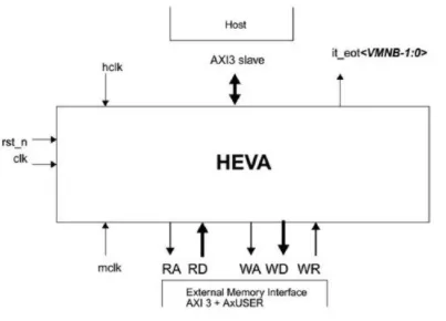
The Hardware Encoder Video Accelerator (HEVA), supports HEVC encoding low complexity with a flexible architecture targeting at least 1080p60 with minimal processing units and memory cuts and
up to 2160p120 with large number of units and large memory cuts.
Trade-off performance/area at design configuration: Reference cache size for 2160p30 at 350 MHz, 1 reference frame and bandwidth, overhead of 100% for references i.e. 1.5 GBytes/sec (minimal is 1.2 GB/s)
Hardware interfaces :Host interface AXI3/AXI4 slave interface for the registers and command/status FIFO, Memory interface AXI3/AXI4 Streaming interfaces to External DRAM, Asynchronous AXI3/AXI4 128 bits interface, Synchronous DMA arbiter and memory interface
Task sequencing modules: Manages communication and storage between processing modules, Control the shared memories and caches between the TPU modules and TSU/MIF, Defines the execution mode of the task processing units
Task processing modules: Perform the pixel and bit-stream processing under control of TCR/TSU, The number of processing elements is defined at design configuration to sustain the required
performance, A local reference cache is needed for performance for some processing units.
Learn more about Video Processing IP core
T2M-IP, the global leader in semiconductor IP cores and technology expertise, is proud to announce the immediate availability of its partner's VESA-compliant DisplayPort v1.4 Rx PHY and Controller IP Cores.
T2M announces the availability of its partner’s Bluetooth V6.0 RF Transceiver IP Core in 22nm ULL and 40nm ULP.
Incorporating BroadR-Reach™ technology for Automotive Excellence, this PHY delivers exceptional performance for automotive and industrial applications, providing a superior alternative to traditional BaseT1 solutions.
Designed to meet the evolving needs of next-generation automotive and industrial applications, the CAN XL Controller IP offers superior performance and flexibility while maintaining backward compatibility with previous CAN standards.
T2MIP, a leading provider of semiconductor IP cores, proudly announces the immediate availability of their partner's H.264 and H.265 HEVC Codec IP cores.
T2M-IP is excited to announce that its state-of-the-art USB 3.0 IP, developed in the 22nm ULP (Ultra Low Power) and ULL (Ultra Low Leakage) process technologies, has been successfully licensed to over 10 customers worldwide in the past two years.