Vendor: Synopsys, Inc. Category: DDR

Gen 2 DDR multiPHY IP

The Gen 2 DDR multiPHY IP cores are mixed-signal PHY IP cores that supply the physical interface to JEDEC standard LPDDR2, LPDDR3…

Controller + PHY + 1 View all specifications

Overview

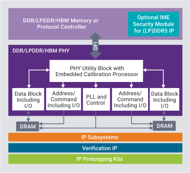
The Gen 2 DDR multiPHY IP cores are mixed-signal PHY IP cores that supply the complete physical interface to JEDEC standard LPDDR2, LPDDR3, and DDR3 SDRAM memories. The Gen 2 DDR multiPHY IP supports the entire range of DDR3 SDRAM speeds, from DDR3-666 through DDR3-2133, LPDDR2 SDRAMs from 0 to 1066 Mbps and LPDDR3 SDRAMs from 0 to 2133 Mbps. The Gen 2 DDR multiPHY IP are compiled into a hard macro that is optimized for specific foundry nodes. Each Gen 2 DDR multiPHY is constructed from the following libraries of components: application-specific SSTL I/O library, a single address/command macro block, multiple byte wide data macro blocks instantiated as many times as required to accommodate the memory channel width and separate PLL macrocells that directly abut to the address/command macro block and data macro blocks.

A key component of the Gen 2 DDR multiPHY is the extensive in-system data training/calibration capability that is used to maximize the overall timing budget and improve system reliability. The Gen 2 DDR multiPHY contains calibration circuits for read data eye training (optimizes and maintains the optimal DQS offset into the center of the read data eye), write data eye training (optimizes and maintains the optimal DQS offset into the center of the write data eye), per-bit deskew training (minimizes bit to bit timing skew for reads and writes independently), DDR3 write leveling, and DDR3 read leveling. The Gen 2 DDR multiPHY also supports per-bit deskew calibration of the address/command bus for LPDDR3 SDRAMs.

Key features

  • Support for JEDEC standard LPDDR2, LPDDR3, and DDR3 SDRAMs
    • Includes support for DDR3L (1.35V) and DDR3U (1.25V) SDRAMs
  • When combined with a Synopsys DDR memory or protocol controller and verification IP, Synopsys provides a complete DDR3/LPDDR2/LPDDR3 interface IP solution
  • Compatible with the Synopsys DDR PHY Compiler
    • GUI-based tool used to assemble a customized DDR PHY targeting a specific application
  • Scalable architecture that supports data rates up to DDR3-2133
  • Support for DIMMs
  • Delivery of product as a hardened mixed-signal macrocell components allows precise control of timing critical delay and skew paths
  • Low latency
  • PHY Utility Bock (PUBM2) included as a soft IP utility that includes control features, such as write leveling and data eye training, and provides support for production testing of the Gen 2 DDR multiPHY
  • DFI 2.1 compliant interface
  • Configurable external data bus widths between 8 and 64 bits in 8-bit increments, plus ECC
  • Permits operation with SDRAMs using data widths narrower than the compiled data width (for example, a 32-bit interface can use just 16 bits to interface to a 16-bit wide SDRAM)
  • Support for 1 to 4 memory ranks
  • PHY-Controller interface runs in 1:1 or 1:2 mode (ratio of application bus clock to SDRAM clock), simplifying core logic timing constraints
  • Includes the PLL and all timing circuits necessary to meet timing specifications
  • Write leveling timing circuits to compensate address and control versus data delays
  • Write and read bit timing circuits compensate per-bit delay skew of individual data bits within each data byte
  • Per-bit deskew of the address/command bus for LPDDR3 SDRAMs
  • Locally calibrated timing circuits minimize OCV and ACLV effects, and accommodate voltage or temperature change induced timing drift
  • Area-optimized I/O
    • 6 layers of metal
    • 25um I/O pitch for 28nm
    • Supports circuit under pad (CUP) and bond over active (BOA)
    • Supports flip chip and wire bond
  • I/O retention mode
    • Maintains I/O drive state during VDD power down
    • Optional CKE retention mode permits VDD and all non-essential I/Os to be powered down while retaining the external SDRAMs in self refresh mode
  • Accommodates any poly orientation in 28nm processes and below, allowing the Gen 2 DDR multiPHY to go around a corner if required
  • Advanced testability
    • At-speed loopback testing on both the address and data channels
    • Delay line oscillator test mode
    • MUX-scan ATPG
  • Optional DDR signal integrity service is available to assist customers with the integration of the PHY into their SoC, package, and printed circuit board environments

Block Diagram

Specifications

Identity

Part Number
dwc_ddr_gen2_multiphy
Vendor
Synopsys, Inc.
Type
Silicon IP
Controller / PHY
Controller + PHY , PHY

Files

Note: some files may require an NDA depending on provider policy.

Provider

Learn more about DDR IP core

Which DDR SDRAM Memory to Use and When

This whitepaper provides an overview of the JEDEC memory standards to help SoC designers select the right memory solution, including IP, that best fits their application requirements.

Synopsys Interconnect IPs Enabling Scalable Compute Clusters

With more than 25 years of experience in delivering field-proven silicon IP solutions, we are thrilled to partner with NVIDIA and the NVIDIA NVLink ecosystem to enable and accelerate the creation of custom AI silicon. This strategic collaboration will leverage Synopsys' expertise in silicon IPs to assist in the development of bespoke AI silicon, forming the foundation for advanced compute clusters aimed at delivering the next generation of transformative AI experiences.

Frequently asked questions about DDR Interface IP

What is Gen 2 DDR multiPHY IP?

Gen 2 DDR multiPHY IP is a DDR IP core from Synopsys, Inc. listed on Semi IP Hub.

How should engineers evaluate this DDR?

Engineers should review the overview, key features, supported foundries and nodes, maturity, deliverables, and provider information before shortlisting this DDR IP.

Can this semiconductor IP be compared with similar products?

Yes. Buyers can compare this product with similar semiconductor IP cores or IP families based on category, provider, process options, and structured technical specifications.

×
Semiconductor IP