Overview
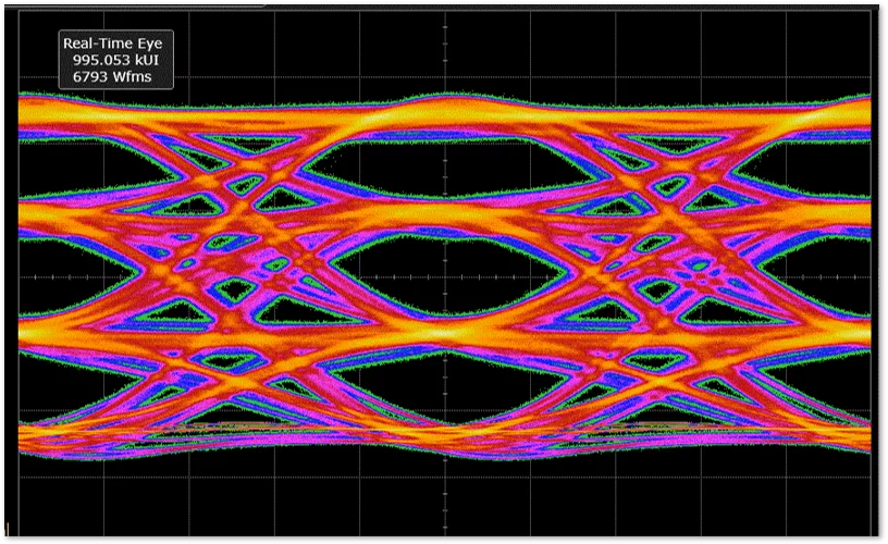
The GDDR6X/6 PHY is fully compliant with the JEDEC GDDR6X/6 standard, supporting data rates of up to 20Gbps per pin for PAM2 GDDR6 mode and 24Gbps for PAM4 GDDR6X mode. The GDDR6X/6 interface supports 2 channels, each with 16 bits for a total data width of 32 bits per memory device. With a maximum speed of 20/24Gbps per pin, The GDDR6X/6 Combo PHY delivers a peak bandwidth of up to 80GB/s or 96GB/s per memory device. Designed for advanced FinFET process nodes, this PHY is optimized for seamless integration into cutting-edge applications.
The comprehensive product portfolio also includes full GDS delivery, signal integrity and power integrity (SI/PI) analysis, verification models, prototyping support, and simulation tools. These offerings empower customers to accelerate development cycles, ensure robust performance, and stay ahead in the competitive landscape of high-performance memory solutions.
Learn more about DDR IP core
INNOSILICON Technology today officially announced the launch of its comprehensive high-speed UALink (Ultra Accelerator Link) solution portfolio, featuring industry-leading single-lane 112G/224G high-performance PHY technology.
Recently, Innosilicon Technology, a seasoned player with nearly 20 years of expertise in the IP industry, has announced a major milestone: its self-developed LPDDR6/5X ComboPHY+controller IP has been successfully signed and delivered to a leading industry client.
At the event, the company will showcase its leadership in ready-to-deploy AI solutions, featuring high-speed memory, SerDes, and chiplet subsystems, with a spotlight on its LPDDR6/5X Combo offering.
Innosilicon, a leading IP provider, offers a complete PCIe 5.0 solution stack that includes both PHY and controller IPs. Although both layers are crucial to achieving a fully compliant and high-performance PCIe interface, this paper deep dives into the technical challenges of PHY design, highlighting insights drawn from real-world design margins, receiver robustness, and advanced jitter analysis in the context of Gen5 systems.
Pioneering the industry, Innosilicon has deployed two fully-compatible upgrade solutions LPDDR5/5X/4/4X Combo IP and DDR5/4 Combo IP across multiple global mainstream 28nm and 22nm process nodes, effectively helping customers tackle supply chain upgrade challenges.
This white paper will discuss the design challenges that IC designers are facing when developing the new GDDR 7 high-performance memory interface and highlight some of the possible solutions to overcome these challenges, ensuring compliance and robustness of the GDDR7 memory interface.