Overview
Latest and forthcoming CMOS image sensors surpass 10M pixels, and output video at 30 and even 60 fps.
This development requires high bandwidth between the camera and the application processor.
For example, a commercially available 4068x3456 30 fps camera outputs an average of over 5Gbps,
which requires 4 DPHY lanes at more than 1.25Gbp – more the original 1Gpbs of MIPI DPHY 1.0,
but still manageable by the extended 1.5Gbps of the latest DPHY spec.
However, when the same or similar camera is introduced with 60fps, over 10Gbps will be required,
and 4 lanes will not suffice.
MIPI’s forthcoming new set of standards (CSI3 over UNIPRO and MPHY) will offer higher bandwidth.
However, until those standards are available, camera vendors are looking for ways to increase CSI2 speed.
Among others, extension of the CSI2 standard to 8 data lanes, with one or two clock lanes, are introduced.
Application processor vendors also face speed issues. Processing frames of 16 million pixel at 60 fps
require the processing of 1G pixel per second. As employing a 1GHz clock is not desirable, the trend is to
process more than one pixel in each clock cycle.
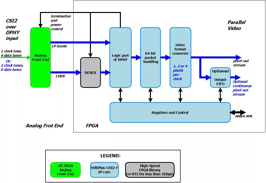
VLSI Plus' SVRPlus-CSI2-F IP core is designed to support those trends, and, at the same time, work with a
relatively slow clock rate, processing several pixels per clock.
The SVRPlus-CSI2-F has an internal 64-bit bus. With this bus width, 10Gbps can be handled by a reasonable 167MHz clock.
The output path of the SVRPlus-CSI2-F can handle 1, 2 or 4 pixels in parallel. Image sensors which generate, for example,
12M * 60 fps = 720M pixels per second, can be handled by the SVRPlus-CSI2-F driven by a 180MHz clock, if the
PARALLEL_PIXELS compilation switch is set to 4.
The SVRPlus-CSI2-F can handle up to 8 data lanes, with one or two clock lanes, and at up to 1.5Gbps per lane.
If extended CSI2 is not required, the customer can save gate count and off-FPGA circuits by setting the EIGHT_LANES
compilation switch to NO.
Learn more about MIPI IP core
The imbalance between I/O speed and internal logic speed in integrated circuits has shifted in recent years in favor of the I/O. While in the past, the performance of integrated circuits was often limited by the I/O rate, today, in both ASICs and FPGAs, internal logic struggles to keep up with the I/O performance.
In this article, we show how fast video streams conforming to MIPI CSI2 rev2.0 over MIPI DPHY rev1.2 can be generated, using VLSI Plus’ SVTPlus-CSI2-F IP core, with simple off-FPGA analog front-end. The high bit rates can be achieved with a relatively slow FPGA clock frequency, trading off FPGA resources for simple timing closure.
VLSI Plus today announced the availability of the CSI2-MUX-A1-F – a MIPI® CSI2 transceiver, connecting to up to 4 CSI2 camera inputs, and outputting a multiplexed CSI2 stream with 4 data lanes, at up to 1.5Gbps per lane.
VLSI Plus today announced at the MWC conference the availability of the SVT-CS4-AP2 – a MIPI® CSI2 compliant serial video transmitter, supporting multiple concurrent video sources, and employing from 1 to 4 DPHY lanes at up to 1.5Gbps per lane.
VLSI Plus today announced the availability of Alias-DT option, which enables outputting multiple pixels per clock, in all its MIPI® CSI2 Receiver IP cores (the SVR family).
VLSI Plus today announced the availability of the SVRPlus-CSI2-F a 64 bit serial video receiver, supporting MIPI® CSI2 and extensions to CSI2 with up to 8 data lanes and two clock lanes, and outputting 1, 2 or 4 pixels per clock.